
For almost three years IBM has been using RFID technology to track thousands of chip orders at its state-of-the-art, automated semiconductor wafer fabrication facility in East Fishkill, NY. The 140,000 sq. ft., multibillion dollar facility, which went operational in mid-2002, is the first fully automated semiconductor manufacturing and development facility in the world. By using RFID technology integrated with production tools, the facility's system can make decisions about what product to run next, how to run it, and when to run it. The plant's operational systems can track individual semiconductor wafers down to the chamber and slot in which they are being processed.
 |
RFID technology identifies where the wafers are in the process and which production assets are needed. Since wafers typically go through hundreds of operations during processing, tracking and optimizing the steps needed for manufacturing is critical.
Wafer Fabrication
The line, which produces advanced processor chips, runs continuously, even when unattended. Silicon wafers are placed in front-opening unified pods (Figure 1). Each FOUP can carry up to twenty-five 300 mm dia. silicon wafers, each of which is diced into integrated circuits at the end of the wafer fabrication process, with as many as a thousand chips to a wafer. As a result, each FOUP can carry thousands and sometimes even millions of dollars worth of finished product—something you wouldn't want to misplace or mishandle.
 Figure 1. Each front-opening unified pod (FOUP), like the one shown here, is a sealed superclean mini-environment opened only at processing ports to load or unload wafers |
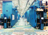
Thousands of these containers on an overhead transport system (Figure 2) move semiconductor wafers between processing stations. They are a key part of the automated system that uses real-time information to optimize the complex wafer fabrication process. Wafers remain locked in the FOUP during the entire manufacturing process, which normally takes about a month. Unless a wafer-manufacturing tool fails, nobody ever needs to physically touch a wafer in the factory.
Where RFID Fits In
Each of the FOUPs, which complies with semiconductor industry standards for 300 mm wafer carriers, is made of a polycarbonate material, embedded with a passive RFID tag written with a unique identification number. These tags can be read by RFID readers located throughout the fabrication facility.
Every processing tool—ranging from lithography exposure tools, chemical etchers, and ion implanters to metal deposition equipment, chemical mechanical polishers, and furnaces—contains an RFID reader. Readers are also strategically located within the transport system throughout the facility. The thousands of RFID readers have a 3–6 in. read distance. The fact that RFID does not require line of sight for reading the tag greatly simplifies design of the system.
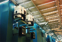 Figure 2. Thousands of FOUPs glide along the overhead transport system that moves semiconductor wafers between processing stations |
The RFID system is used to track the FOUPs as they travel throughout the facility. Each time a FOUP is loaded with a new set of wafers, the FOUP's RFID identity is read and the wafer barcodes are correlated with the carrier's ID using IBM DB2 Universal Database. An IBM manufacturing execution system, SiView Standard, then coordinates information between IBM Websphere middleware and DB2 to automatically control and optimize each step of the fabrication process.
Between 5000 and 6000 FOUPs are in circulation at the IBM plant. Wafers can be added to or removed from a FOUP during the fabrication process, and each FOUP travels a different route based on the products being run and on operating conditions. If the process is running well, the system may choose to eliminate certain feedback steps; if the process needs additional feedback, it will automatically trigger those steps.
The system also automatically determines optimal wafer processing sequences based on incoming customer orders. If a customer orders X number of wafers by a certain date at a certain priority level, that information is fed directly into the factory system. Using real-time order information, the system then creates a factory schedule to ensure the delivery of commitments made within the supply chain. This schedule then optimizes each lot delivery.
The Benefits
IBM lists improved factory performance, enhanced employee productivity, and more responsive customer service among key benefits of the East Fishkill automated system. The plant can operate with fewer employees than would otherwise have been needed, and product errors and delays are reduced due to the decreased need for human intervention. Full automation makes the plant more efficient—it can help spot potential problems earlier—and more flexible when it comes to producing multiple chips.
Thanks to the availability of real-time processing data gathered through RFID, customers can check the status of their microchip orders within the plant through a Web-based portal system called Customer Connect. Further, in the case of problems with chips in the field, the system provides the ability to trace the processing steps performed on the product back to the individual tools used, and the time that each processing step was performed.
The use of RFID is fundamental to enabling superior traceability and control during the complex fabrication process. RFID is the best tool to manage wafer production. The programmable chips carry information about each wafer's requirements and the RFID readers throughout the plant provide information should a course correction be required. IBM plans to expand the use of RFID in its Fishkill facility and other plants worldwide to manage production as well as to track IT assets, backup and recovery services tapes, and shipping containers used to move computer servers between sites.
Ann Breidenbach can be reached at IBM Corp., Somers, NY, 914-766-1970, [email protected], www.ibm.com