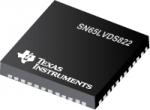
The SN65LVDS822 FlatLink LVDS receiver exploits a modern CMOS process to deliver
several unique features. These include three selectable CMOS output slew rates, CMOS output voltage support of 1.8 V to 3.3 V, a pin out swap option, integrated differential termination (configurable), an automatic low-power mode, and deserialization modes of 4:27 and 2:27. The device integrates five low-voltage differential signal (LVDS) line receivers: four data lanes and one clock lane. The clock is internally multiplied by 7 or 14 (depending on pin MODE14), and performs sampling of LVDS data. Additionally, the device operates in either four-lane 7x mode, or two-lane 14x mode. Each input lane contains a shift register that converts serial data to parallel. A datasheet is available at http://www.ti.com/lit/ds/symlink/sn65lvds822.pdf.
Texas Instruments Inc.
Dallas, TX
972-995-2011
512-434-1560
http://www.ti.com
Contact Info