
There is a long history of research and development in the field of wireless sensors, with many of the attempts aimed at eliminating cabling in the manufacturing environment. The high cost of installation, the high failure rate of connectors, and the difficulty in troubleshooting connections are just some of the factors driving users to investigate alternatives (see the sidebar “Bluetooth,”).
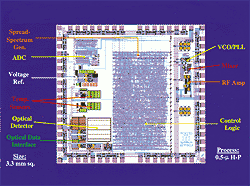 |
| Photo 1. Oak Ridge National Laboratory’s second-generation integrated wireless sensor has both onchip and offchip sensor capabilities. The optical data port provides a wireless interface for changing gain, update rate, and other parameters using a TV remote control instead of jumpers. This is part of its migration to a fully bidirectional telesensor chip. (Photo courtesy of Oak Ridge National Laboratory.) |
The current use of bus architectures (e.g., Ethernet) is an attempt to address some of the inherent problems associated with wiring a plant. But companies find that many installations are simply impossible without eliminating the tether of the communications and power lines. Other applications require such widespread and diffuse sensor placement that running wires makes the cost of installation prohibitive.
A new paradigm is emerging, though, in which sensors are integrated with signal conditioning, digitization, intelligent processing, and communications components—all on the same silicon substrate (see Photo 1). Add radio telemetry to the mix as the communications medium, and you have a new generation of sensors that overcomes the limitations associated with wiring (see the sidebar “You Can Get Them Here,”).
The utility of wireless sensor technologies is expected to affect many aspects of plant operation, most notably those applications that benefit from the deployment of many sensors or networks of sensors. The engineering community can then perform context-dependent anticipatory maintenance and system health monitoring at the plant or enterprise level because of the elimination of the infrastructure costs associated with wiring. The door will be open to paradigm shifts in sensor deployment philosophy, including process flow-through sensors (inside-out sensing vs. outside-in), peel-and-stick devices, and embedded-and-shipped systems that can be remotely accessed via the Internet.
| Bluetooth |
| According to industry analysts, Bluetooth could well become the fastest growing de facto networking standard. Experts predict that before 2002 Bluetooth’s wireless technology will be built into millions of electronic devices. Following in the footsteps of Ethernet, which was once thought to be inappropriate for industrial applications, Bluetooth may prove to be as suitable for industry as it is for home and office. The original Bluetooth consortium consisted of Nokia, Toshiba, IBM, Intel, and Ericsson. With major players like Motorola, Philips, and Hewlett-Packard joining the current 1100 participants, most people agree that the emerging standard will have a huge impact in the marketplace. An evaluation kit is available from Ericsson (www.ericsson. com/microe) for about $15,500 for those who want to get started developing products immediately. The first real product, expected from Ericsson in mid-2000, will be a 2.45 GHz wireless headphone set for mobile phone users. Total worldwide Bluetooth sales are projected to be more than $2 billion by 2005. The Bluetooth specification (which builds on the existing IEEE-802.11 wireless LAN standard) represents a key milestone in providing open standards for wireless communications. The T2901 transceiver (samples available) implements the standard with 1.0 mW output power in the 2.45 GHz ISM (industry, scientific, and medical) band. The protocol provides 1600 frequency hops per second among 79 channels and supports a maximum data rate of 1.0 Mbps. Pseudo full-duplex operation is achieved through a time division multiplexing scheme. Performance in an industrial environment is yet to be investigated. More details about the Bluetooth specification can be obtained at www.bluetooth.com. Some Bluetooth competitors also exploit the IEEE-802.11 wireless Ethernet standard. HOP and SWAP are the two closest competitors challenging the Bluetooth consortium. |
Enter the Department of Energy
The significance of wireless technology to leading national industries has not eluded the federal government (see the sidebar “Uncle Sam Invests in Wireless,”). In 1997, the President’s advisers on science and technology asserted that the development of wireless sensors could improve production efficiency by 10% and reduce emissions by more than 25%.
In 1999, the Department of Energy’s (DOE’s) Office of Industrial Technology (OIT) established the Sensors and Controls (S&C) Program to take steps that would advance the development and deployment of integrated measurement systems for operator-independent control of manufacturing processes with applicability across a broad range of industrial sectors. The program serves the agriculture, aluminum, chemical, forest products, glass, metal-casting, mining, petroleum, and steel industries. All nine have established individual partnerships with DOE to collaborate in joint technology development aimed at enhancing the competitiveness and vitality of the industries.
The Project. The S&C Program’s current project is to demonstrate the feasibility of wireless sensors in a real manufacturing environment and to provide a test bed for third-party suppliers to evaluate their products. Working at the Oak Ridge National Laboratory (ORNL) in Oak Ridge, Tennessee, the project team is developing a scheme to achieve reliable data telemetry in industrial environments. As the architecture and hardware matures, integration of various sensor technologies—including legacy systems as well as emerging technologies (e.g., MEMS-based microsensors)—will be implemented.
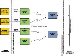 |
| Figure 1. Oak Ridge National Laboratory’s project must support connectivity from existing transducers to legacy networks. Early tests will include three sensor nodes and two network nodes. If a sensor node loses connectivity to a specific network node, another network node will pick up the connection and maintain connectivity. |
Requirements. For this project, the systems must operate with minimum operator intervention. For a wireless network, this translates to a system that is self-starting, self-configuring, and self-healing. In addition, the architecture must support existing (legacy) sensor systems. The approach here is to embrace existing standards—such as those for smart sensors (IEEE-1451) and Ethernet (IEEE-802.3)—but still be able to work with other protocols as necessary. Finally, the system must be able to operate in the harsh environments common to these industries.
The Architecture. Maintaining connectivity in a plant requires attention to the temperature, vibration, electromagnetic, and humidity conditions during both storage and operation of the devices being deployed (see Figure 1). The dynamic nature of the environment affects the design constraints because changing conditions are inherently more difficult to predict. Critical assumptions must be made about the environment for the design to be viable. Those assumptions are based on representative conditions found in existing industrial plants and facilities.
Demonstrated connectivity in the network is insufficient to ensure a viable system. Connectivity must be verifiable without major impact on the performance of the system and without significant personnel training or additional tools. Verification must involve consideration of such issues as headroom, error rates (corrected and uncorrected), and latencies. In the user mode of this system, only data coming from sensor nodes (SN) or network nodes (NN) are available to you. In the super-user mode, the device (i.e., an SN or an NN) can be interrogated and forced into a mode that stresses the network for diagnostic purposes.
| You Can Get Them Here |
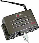
Computational Systems, Inc. (CSI), a small company in Knoxville, Tennessee, recently announced the availability of the first fully integrated wireless sensor for use in the rugged environments common to manufacturing. Its device—which is about the size of a soda can—measures critical operating parameters (e.g., temperature and vibration) of machines and reports back to a central host, which integrates information from a number of the sensors and provides reports. announced the availability of the first fully integrated wireless sensor for use in the rugged environments common to manufacturing. Its device—which is about the size of a soda can—measures critical operating parameters (e.g., temperature and vibration) of machines and reports back to a central host, which integrates information from a number of the sensors and provides reports. CSI’s proprietary architecture addresses many of the critical issues that characterize a viable industrial network. Devices can act as repeaters and can coexist with a large number of cooperating sensors. CSI, now a wholly owned subsidiary of Emerson Electric, can be reached by phone at 865-675-2110 or through its Web site: www.compsys.com. Grayhill, Inc., located in La Grange, Illinois, is a traditional supplier to the manufacturing marketplace that has partnered with an OEM radio supplier to provide a wireless network interface compatible with its product line. The device, the EZCom wireless LAN transceiver, offers wireless Modbus connectivity in a rugged package suitable for manufacturing environments. The 900 MHz transceiver incorporates many spread spectrum features that make the new generation of wireless interfaces robust enough for industrial environments. For more information, go to www.grayhill.com/products/ ezcom or call 708-354-1040. |
Unidirectional SN devices must implement a publish/subscribe protocol that lets you verify the operation of the sensor. The maximum latency in the verification protocol is application dependent and is set when the sensor is deployed. Bidirectional SN devices support protocols that provide faster verification of operational status. In this case, the master/slave mode is the preferred form of operation. With this protocol, the maximum latency is set by the master.
Accidental or purposeful interference (either by individuals or other hardware systems) can affect connectivity. To avoid disruption of operations, the security system is designed to handle all potential interactions. To this end, the security implementations are graded and role-based. For instance, with the user mode, you have less authority than you would with the super-user mode. The developer mode provides the highest level of access. But before you can use it, you must set the device to an offline state.
Security implementations focus on providing cost-effective protection against the most likely scenarios. Additional security can be added to prevent greater threats to performance. Implementation of the security measures is as transparent as possible so that normal, authorized access to the system continues unimpeded while unauthorized (or unintended) access elicits immediate and terminal actions. Super-user access can override automatic security features.
Data encryption between an SN and an NN depends on the application. The natural encryption provided by the code division multiple access (CDMA) protocol, implemented in the over-the-air link, is the minimum supported. You can supplement the encryption to meet the needs of your application. Error-detection and -correction protocols provide a corrected bit error rate (BER) of 10–9. Dynamic adjustments of the BER for maximum throughput are permitted if suitable procedures are in place to meet the standards under all conditions.
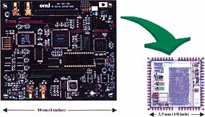 |
| Photo 2. Migration from board to chip requires careful design at the board level so that the transition to the chip meets the desired power, size, and functional goals. Ultimately, we will add bidirectional RF capability and sufficient intelligence to avoid the need for high-bandwidth communications. |
Configuration management is simple and fast. Temporary interruptions of connectivity are immediately (within about 1 s) mitigated through reconfiguration and rerouting. These corrective measures are initiated by the normal dynamics of the environment or the system and do not require human intervention. Failed devices (SN or NN) are reported quickly. A failed SN could result in loss of sensor data unless a different NN can derive the measurement from other sensors and provide the new measurement as a substitute. A failed NN will cause the existing NNs to reconfigure to intercept the signal from the orphaned SN and provide the sensor data to the network. Notification of the event will be controlled so that a rash of events won’t result in a flood of network activity reporting the event.
The system supports the 4–20 mA analog sensor interface. This allows a load that can be used to power an SN device. The system implements the IEEE-1451 protocol in the SN device, which will include the definition of suitable data structures. The first NN devices implement an Ethernet interface to the plant backbone. The actual hardware implementation (e.g., thin wire or RJ-45) will be determined later.
Design. The design criteria had the project begin with simple devices that meet the critical requirements but ultimately have a migration path (see Photo 2) to devices implemented in one (or a very few) ASIC. Early attempts to produce single-chip solutions provided important research results but were not as useful to the customer because critical testing was never done on the underlying architecture.
The telemetry portion of the project was designed to be modular and adaptable so that developers of IEEE-P1451.3 systems could use it as a reference design for future applications. Both the software and hardware have been designed in a fashion that allows rapid prototyping of tailored applications. In fact, the design of the system is helping to define the details of the IEEE-P1451.3 protocol by allowing committee members to see the effects of protocol decisions as they are being made.
| Uncle Sam Invests in Wireless |
| Several federal agencies actively support efforts to develop and deploy wireless technology. The Defense Advanced Research Projects Agency (www.darpa.mil) has long been involved in promoting the growth of wireless sensor technology for the military. Rockwell International is a key industrial partner, with its Wireless Intelligent Network of Sensors program (www.wins.rsc. rock well.com). The Department of Commerce—through the National Institute for Standards and Technology—has a program called Smart Spaces, which also promotes the technology. And the Department of Energy’s Office of Industrial Technology (OIT) sponsors the Oak Ridge National Laboratory’s research in the field. These are just a few of the programs supported by the government. |
The RF portion of the design incorporates a fairly standard heterodyne receiver topology and a direct up-conversion transmitter—both operating in the 902–928 MHz band. The first version is a QPSK (quadrature phase shift key) half-duplex system that typically is in receive mode but disables the receiver for the duration of the burst transmissions.
The design includes a programmable digital synthesizer that will accommodate all typical frequency bands and a voltage-controlled oscillator that covers the frequencies of interest using a tuning voltage range of 0 VDC to 5 VDC. The front-end RF/analog components must be linear and offer reasonably wide bandwidth to handle the CDMA applications. For example, a data rate of 50 Kbps and spread-spectrum coding length of 63 bits (chips) would require a double-sided RF bandwidth of (50 k ¥ 63 ¥ 2), or 6.3 MHz. Also, the automatic gain control (AGC), the mixer, and other components have to be very linear to prevent distortion of the CDMA signal.
Another key feature of the design is that it is a coherent receiver. While many systems accomplish coherency through analog means, this process is performed digitally inside a Stanford-Telecom STEL-2000A chip. The final down-conversion from an intermediate frequency (IF) of about 11 MHz to a baseband signal uses a numerically controlled oscillator (NCO) as the final local oscillator (LO). Feedback of the correlator output allows the NCO to be locked to the incoming digitized IF signal. All receiver processing upstream of this point is accomplished with an analog LO, a mixer, and an AGC. The downstream processing includes a digital matched correlator that despreads the data, combines the quadrature data into a single stream, and performs the differential decoding.
The message-processing portion of the design includes a microprocessor that provides node processing as well as interfacing functions. It also includes a field-programmable gate array that is used to parse the decoded stream from the STEL-2000A and determine the quality of the packets before they are passed to the node processor.
The digital portion of the circuit is set up to accommodate both SNs and NNs. If the hardware is used as an NN, a Hewlett-Packard network-capable application processor (NCAP) and a custom daughterboard are attached to a digital circuit developed at ORNL. The daughterboard has parallel STEL-2000A ICs that let the network decode truly simultaneous CDMA transmissions from the sensor nodes.
If the same hardware is used as an SN, the NCAP and daughterboard are omitted, and a small section of the same PCB is populated to accommodate the 4–20 mA transducer input.
Performance. The first implementation of the wireless communications module is expected to operate at a level of performance consistent with the basic needs of the candidate industries. A throughput of 50 Kbps over the untethered distance of 50 m will meet the initial requirements. As the design matures, the throughput is expected to improve to more than 1 Mbps over about the same distance. The power demands will decrease as the design moves from discrete components to more and more dedicated ASICs. The architecture requires that any link experiencing difficulties should be remapped to maintain connectivity suitable for the real-time needs of the target industries.
Conclusion
The DOE/OIT project will provide prototypes that verify the feasibility of moving toward wireless connectivity for the target industries. The goal is that industrial partners joining the project will commercialize the products, providing devices, components, and systems suitable for industrial applications at a reasonable cost. This will open new markets and opportunities that will, in turn, motivate improved technologies and reduced costs. The ultimate outcome will depend, however, on many technical, social, and marketing forces.
The systems and components resulting from this project will first see the factory floor in the summer of 2000. Once the project has demonstrated the viability of the architecture and protocols, it will begin to migrate toward more integrated (compact) solutions. Project participants are currently soliciting partners who want to test/adapt the networks for use in their own facilities. Under suitable financial arrangements, the project will have the devices it prototyped duplicated, installed, and tested in a partner’s site and provide written reports on the performance. The underlying architecture and protocols will remain open with special licensing available for any other intellectual property included in the implementation.
The next generation of components (available in 2001) will provide improved performance, lower power demands, and improved dynamic remapping performance. The Oak Ridge National Laboratory test bed will continue to be available for use by third-party suppliers or end users to verify operation of new devices and systems.
The work of the project will generate a number of long-term benefits, including greater embedded intelligence, which will allow cooperating sensors to assume more of the responsibility for process optimization. The first new devices will use innovative techniques to provide feature abstraction, information abstraction, and finally knowledge-level abstraction. The key goal of the program will continue to be the implementation of these technologies in a form suitable for use in the targeted industrial environments.
Authors’ Note
The best way to keep up with what’s happening with wireless technology is to search the Web from time to time. A number of online newsletters are available as no-cost subscriptions, including Wireless Design Online.