

Embedded Learning
If any platform seems to be all-encompassing, embracing and exploiting every area of technology from simple consumer appliances to complex data analytical systems and medical devices, it's that ever mentioned and constantly looming platform called the Internet of Things (IoT). It's probably safe to say the IoT is here and any developments within can be considered its evolution. Just a few topics we can sandwich under that umbrella of IoT evolution are artificial intelligence, virtual reality, and deep learning. Such is the focus of NVIDIA's latest embedded offering.
The Jetson TX2 is a credit card-sized board that performs computer vision, deep learning, and an array of embedded artificial intelligence tasks (see figure 1). It is offered as an upgrade to the company's Tegra K1 system-on-chip (SoC) based Jetson TK1 and the Tegra X1-based Jetson TX1.
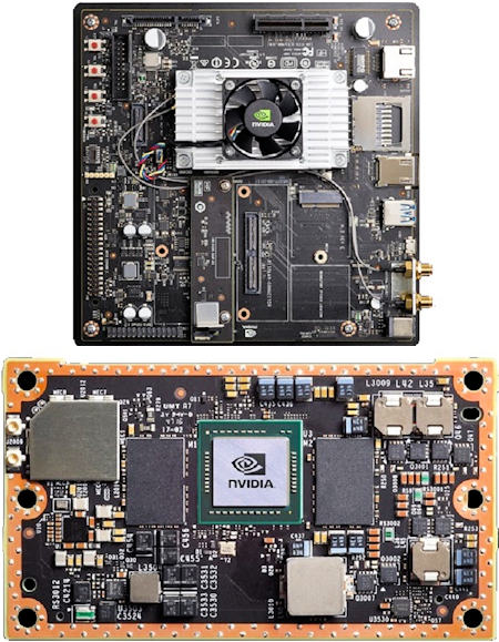
Fig. 1: Jetson TX2 employs NVIDIA's Tegra SoC, based on 64-bit "Denver 2" and ARM Cortex-A57 CPU cores along with a Pascal-generation GPU. TX2 comes in a developer kit (top) and production module (bottom) formats.
Production
The production module employs what the company refers to as a "Parker Series SoC. Essentially, its application processor's specs are comparable a SoC.
The Jetson TX2 production module operates in two modes: Max-P (maximum performance) and Max-Q (maximum energy efficiency). In Max-P mode, the board churns out as much as 2X the computational performance of the Jetson TX1 while consuming less than 15W of total module power. Inversely, operating in Max-Q mode, it exhibits up to 2X the energy efficiency of the Jetson TX1 at less than 7.5W of total module power.
Also in Max-P mode, the SoC's GPU runs at 1,122 MHz and the CPU clusters run at 2 GHz when either the Denver 2s or ARM Cortex-A57s are active or 1.4 GHz with both clusters running simultaneously. In Max-Q mode, the GPU runs at 854 MHz and the ARM Cortex-A57 cluster runs at 1.2 GHz with the Denver 2 CPU disabled.
Partners
Developing a variety of IoT applications is a key feature of the Jetson platform. For example, it has enabled Cisco integrate artificial intelligence (AI) features like facial and speech recognition into its Spark products.
Operating in Max-P mode, the Jetson TX2 module successor is able to allegedly double the number of video decodes and encodes and the number of concurrent DNNs and objects capable of being tracked concurrently. It does all this while consuming just 12W of power.
Preferred Modus Operandi
NVIDIA's production module is the company's preferred hardware approach for the majority of users because it enables the company to deliver regular upgrades to its Jetpack SDK based on a known hardware bill-of-materials. Jetpack recently got an upgrade to v3 alongside with the Jetson TX2 release (see figure 2).
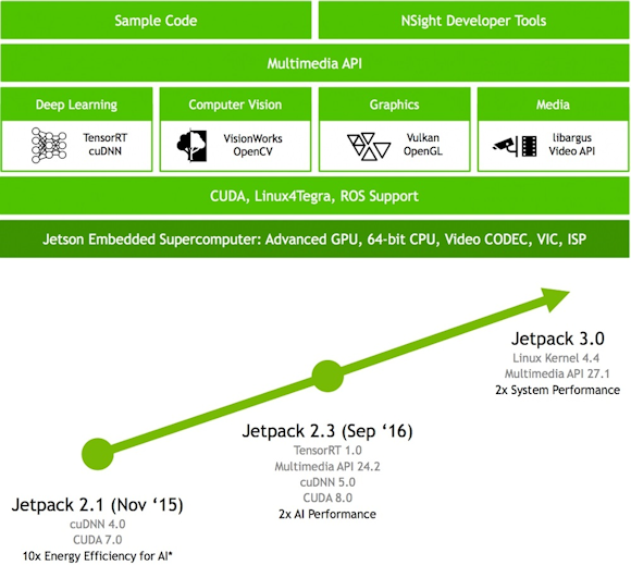
Fig. 2: Jetpack SDK bundles software tools for developing computer vision, AI, and other apps for Tegra SoCs (top). Version 3.0 makes advancements in several key SDK elements (bottom).
For more details on NVIDIA's Jetson platform, here are a few resources to check out:
Next page
DSP Core Ready For 5G And Now
Debuting at Mobile World Congress, CEVA's XC12 is the company's latest DSP core for communication infrastructure applications. The device, considered a major upgrade, is tailored for the bandwidth, latency and user count requirements of emerging 5G cell-supportive infrastructure. This is equipment ranging from remote digital front-end radio heads and multi-mode baseband processing in various-sized base stations to wireless backhaul units. For use in the now, the XC12 also supports current 4G LTE and 802.11 Wi-Fi.
5G Hurdles
The latest 5G draft specifications offer some significant challenges to hardware makers. For example, MIMO antenna array configurations, 3D beam-forming to any particular user, and an 8x latency reduction target for 5G versus LTE. A range of broadcast frequency bands from 400 MHz to millimeter wave-based 80 GHz require support in a full 5G implementation and 256- and 1024-QAM demodulation.
Opps
Volume opportunities exist immediately for the XC12 core. In advance of 5G, cellular carriers are planning rollouts of LTE Advanced Pro, capable of Gbit download speeds. The U.S. FCC also ratified the LTE-U specification, which allows for LTE operation in the 5 GHz unlicensed frequency band currently inhabited by Wi-Fi.
Regardless of the rollout and ramp schedule for 5G, CEVA's Business Development Director for Wireless and Wireline Communications Emmanuel Gresset sees existing technology evolutions and new technology revolutions begging for a DSP upgrade and, according to Gresset, the X12 delivers on these aspirations. This relates to the fact that it is forecasted to run at up to 1.8 GHz on a 10-nm process foundation, translating to 920 GOPs of peak performance, an up-to-8x boost compared to the XC4500 (see figure 3).
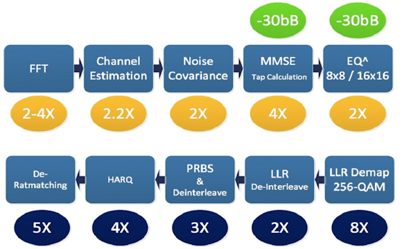
Fig. 3: Combining higher clock speeds, a versatile instruction set, and other architecture advancements, the XC12 can deliver notable performance and other improvements versus the XC4500, according to CEVA.
Architecturally Speaking
According to its maker, the XC12 architecture is a combination of evolutionary and revolutionary advancements versus the XC4500 predecessor (see figure 4). In addition to a larger vector processing unit design, numerous additional dedicated instructions and associated hardware function blocks have been added. These are necessary to support operations required by 5G and other communications standards.
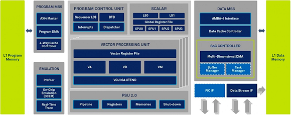
Fig. 4: The XC12's vector processing units are descendants of those in the XC4500 and new scalar units signify a more revolutionary advancement.
With respect to the new core's floating-point facilities, each vector unit includes support for a focused set of both single-precision and half-precision floating-point arithmetic operations. The combination of high-precision fixed and floating-point arithmetic allows for up to 256x256 matrix processing (implementing massive MIMO, for example). Each scalar unit also optionally supports an IEEE-compliant single-precision floating-point unit.
For more details, visit:
XC12 DSP CORE
XC-4500 DSP
5G Specs
About the Author
Mat Dirjish is Executive Editor of Sensors magazine. He can be reached at [email protected].