
According to a new report from market research and consulting firm NanoMarkets LLC (www.nanomarkets.net), the unique electrical, thermal, and physical properties of carbon nanotubes (CNTs) will create $3.6 billion in new business for the electronics and semiconductor sectors by 2009. NanoMarkets' research indicates that carbon nano-tubes are already becoming a key enabling technology that electronics firms should not dismiss as being futuristic.
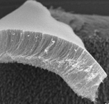 Grass-like multiwall carbon nano-tubes are grown on a silicon wafer and scraped off with a blade to form a freestanding film. Photo courtesy of Dean Aslam, Michigan State University. |
The report, "Carbon Nanotube Electronics, A Technology Analysis and Market Forecast," says that the biggest near-term opportunities for "nanotube electronics" will come from the sensor, display, and memory sectors. Each of these markets will include more than $200 million in CNT-based products by 2007. Nanotubes are already being used to produce tiny sensors, potentially capable of distinguishing a single molecule. This could make nanotubes the material of choice for the highly sensitive sensors required for medical and homeland security applications. The low power consumption of nanotube sensors also makes them an ideal choice for battery-powered sensor networks.
NanoMarkets also notes that CNT-based interconnects and thermal management could serve as an enabling technology for CMOS as it moves to 45 nm and 22 nm nodes. Nanotube-based logic, processors, interconnects, and thermal management solutions are already the subject of intense research by IBM, Intel, and NEC, who believe that their work in this field will help CMOS scale to smaller feature sizes.