
Many sensor applications require high absolute accuracy and linearity, with very low noise, offset, and gain errors over time and temperature. Some example sensor applications that require high absolute accuracy and linearity include magnetic flowmeters, ECG or EEG, and weight scales that produce very small outputs in the µV or mV range. Historically, a sensor analog front end (AFE) can be designed using discrete components such as differential amplifiers and analog-to-digital converters (ADCs). Now the AFE can be incorporated into a single IC, making the system design compact and less complicated for the system designer. Having an integrated AFE means that correcting for signal path errors such as offset and gain errors falls into the hands of the IC designer rather than the system designer. There are many signal path errors, such as noise, linearity, offset, and gain errors. Noise can be reduced through averaging and filtering techniques and designers can compensate for linearity using mathematics. There are also many ways to implement an integrated offset and gain error correction method. This article discusses an effective technique that minimally impacts the sampling channel and ADC's output data rate and is called true continuous background calibration.
In the conventional offset-calibration method, differential inputs to the ADC are internally disconnected from the input pins and then shorted with each other. The offset coefficient is calculated and stored in a register. During the ADC's operation, the offset error from each conversion can be removed by subtracting this coefficient from the digital output code. Similarly, the conventional gain calibration method starts with applying a positive full-scale reference voltage to the differential inputs of the ADC. The gain coefficient is calculated and stored in a register, and then the offset-corrected digital output code is multiplied by this factor to perform gain calibration. However, when using these calibration techniques, the ADC input has to be interrupted while the ADC calculates the offset or gain coefficients. This effectively reduces the ADC's output data rate by up to a factor of six.
True continuous calibration can adjust for the offset and gain errors with minimal impact to the ADC's output data rate. An important assumption behind this calibration technique is that the input is DC, so that any two consecutive samples could be the same. First, let's discuss how to find the gain error coefficient, assuming that there are two gain blocks in the signal path: a fixed-gain amplifier (FGA) and a programmable-gain amplifier (PGA) as shown in Figure 1.
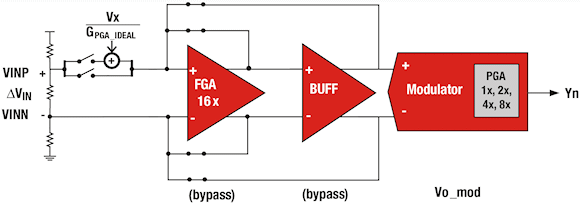 Figure 1. PGA calibration technique diagram |
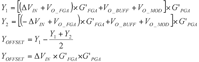
Gain calibration for the PGA (for gains of 1, 2, 4, and 8 times) in the modulator is done by bypassing the FGA and buffer blocks in Figure 1. The first output, Y1, is the multiplication of the PGA gain coefficient, G'PGA, with the differential input, ΔVIN, and the modulator offset voltage, VO_MOD. Using Equation 1 we obtain a ratio of a known and internally generated voltage, VX, and the ideal PGA gain, GPGA_IDEAL. The second output, Y2, is obtained by multiplying G'PGA and the sum of this ratio, ΔVIN, and VO_MOD. The PGA gain calibration is the difference of output codes Y1 and Y2 which is then divided by the ratio of VX and GPGA_IDEAL. Finally, we correct for the PGA error by multiplying the digital output code by G'PGA.
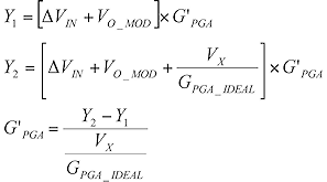 |
(1) |
where:
| Y1 | = | first output code |
| Y2 | = | second output code |
| G'PGA | = | PGA gain coefficient |
| GPGA_IDEAL | = | the ideal PGA gain |
| VO_MOD | = | modulator offset voltage |
| VX | = | internally-generated voltage |
| ΔVIN | = | differential input |
Figure 2 shows the method used for the FGA gain calibration. The gain error for the FGA is eliminated by taking the output codes at alternate samples when the FGA is either OFF or ON. When the FGA is OFF, we capture the difference of the output codes and divide it by two. When the FGA is ON, we do the same, capturing the difference between the two output codes and dividing by two. The gain calibration coefficient, G'FGA, is the ratio of these results as shown in Equation 2. The digital output code is then multiplied by G'FGA to correct for the FGA error.
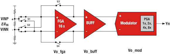 Figure 2. FGA calibration technique diagram |
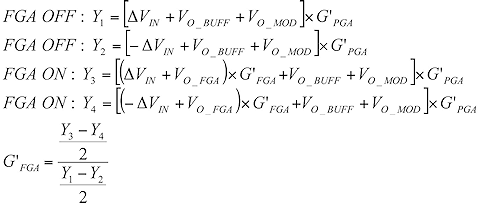 |
(2) |
where:
| VO_BUFF | = | buffer offset voltage |
| VO_FGA | = | FGA offset voltage |
| Y3 | = | third output |
| Y4 | = | fourth output |
For offset error (ΔVIN) correction, we internally reverse the polarity of the alternate input samples at the FGA input as shown in Figure 3. We can obtain the offset calibration coefficient, YOFFSET, by averaging any two consecutive digital output codes, then subtracting this value from the first digital output code using Equation 3. This coefficient can be subtracted from the digital output code to remove the offset error.
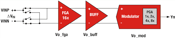 Figure 3. Offset calibration technique diagram |
 |
(3) |
To meet the needs of the many sensor applications that require very low offset and gain errors over time and temperature, we can implement the true continuous background calibration technique. This calibration feature is available in Texas Instruments' family of sensor AFE products. For example, a 24-bit Δ-Σ ADC with multiple channels and low power consumption such as the LMP90100 uses true continuous background calibration to adjust for offset and gain errors. This creates minimal interruption to its sampling channel and ADC output data rate.
ABOUT THE AUTHOR
Amy Le is an applications manager working for TI's Precision Signal Path Business Unit, Santa Clara, CA. Amy can be reached at [email protected].