
Several giant tech companies have joined hands to promote an open standard for chip components called chiplets and how they are crammed together in system-on-chip (SoC) designs deemed critical to a variety of future handheld and high-performance computers that power AI applications and much more.
The open standard, called Universal Chiplet Interconnect Express (UCIe), has been developed by Intel and clearly benefits Intel’s integrated device manufacturer (IDM) strategy as it builds new chip fabs in Arizona and Ohio and elsewhere outside the U.S. Intel has been a prominent voice in the push to expand chip manufacturing outside of Taiwan and the rest of Asia where it is heavily focused today.
“This is an important step forward, and not just for Intel,” said Jack Gold, an analyst at J. Gold Associates. “Some might say that Intel invented this tech and by making it available to everyone, it is self-serving. Does it help Intel? Sure. It is also a major benefit to the whole industry. Many technologies that Intel made have helped them such as USB, and the PCI bus, but they are also industry standards now that everyone has benefited from.”
Intel has donated its UCIe standard to founding members in a new consortium that includes Intel along with Advanced Semiconductor Engineering, Taiwan Semiconductor Manufacturing Co., AMD, Arm, Google Cloud, Meta, Microsoft, Samsung and Qualcomm. The founding group is significant because it includes major competitors to Intel such as AMD but not, so far, Nvidia. Gold said he suspects Nvidia will eventually join at some point.
Notably, the founding members range across cloud, foundries, silicon IP and chip designers. The founders are finalizing terms of incorporation as an open standards body, expected to be completed in third quarter this year. Once incorporated, the group will define the specifics of the chiplet form factor, its management and enhanced security and other protocols.
The founders have already ratified UCIe 1.0 which covers the die-to-die physical layer, die-to-die protocols and software stacks which leverage the existing PCI Express (PCIe) and Compute Express Link (CXL) industry standards.
Intel’s Debendra Das Sharma, chief architect for I/O technologies, has written a white paper on UCIe available for download. In it, UCIe is described as “offering high-bandwidth, low-latency, power-efficient and cost-effective on-package connectivity between chiplets.” There is potential to address projected demands of compute, memory, storage and connectivity across cloud, edge, enterprise, 5G, automotive, high-performance computing and handheld segments, the whitepaper adds.
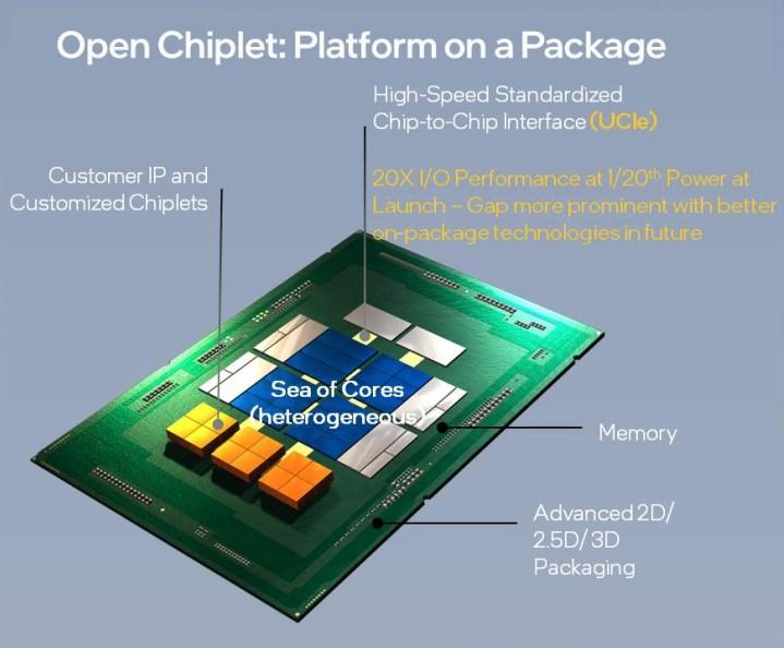
Intel in a statement on Wednesday deemed UCIe as an open specification that defines the interconnect between chiplets within a package such as an SoC, thereby “enabling an open chiplet ecosystem and ubiquitous interconnect at the package level.”
The ability to integrate multiple chiplets in a chip package will deliver future innovations and “is the future of the semiconductor industry,” said Sandra Rivera, executive vice president and general manger of the datacenter and AI group at Intel. Such capability is a “pillar of the Intel’s IDM 2.0 strategy,” she said.
Members of the UCIe consortium will work “toward a common goal of transforming the way the industry delivers new products,” Rivera added.
Gold said the next generation of SoCs will require chiplets from various vendors that can be applied for a standard device or even a custom SoC. “The customization piece is a huge reason why this UCIe is so important,” he said. “It lets specialty components be included much as you do today on a PC board.”
He compared UCIe to how computers are built today with standard buses that let companies pick and choose board level components or backplane comonents to plug in. “The same is moving to the SoC world,” Gold said.
Further, UCIe will significantly reduce development time of new SoCs, since components like network interfaces and video can be reused and don’t need to be redesigned each time a new chip process node is developed. “It makes it much easier to redesign and enhance devices and shortens time to next-generation products,” Gold explained. A company could use older processes such as 20 nm chips for older chiplets without impacting the yield on new processes, such as 5 nm.
Intel will benefit from the UCIe standard “but so do all of the foundries,” Gold said. In theory, “you could grab a chiplet produced at any foundry and then assemble it on a substrate on any assembly location…It’s very much like Nvidia or AMD building a graphics card and being able to plug it into a Dell or HP computer because there is a standard interface, PCIe.”
In another potential example, Samsung could buy a chiplet from Intel and then build out an SoC with the Intel processor but with Samsung components like memory, 5G modems and other parts. Or Samsung make the processor chip interchangeable with an ARM device while keeping all the other components on the SoC the same.
“In theory, this UCIe is a benefit to all chip makers,” Gold said. If UCIe makes it easier to produce chips, it could make it easier to build more fabs in geographies around the globe, a partial answer to a big concern of the semiconductor industry about the need to spread out chip production beyond Taiwan and the rest of Asia where it is heavily concentrated now and where geopolitical threats loom large.
Making it easier to produce chips would heavily benefit countries like India and several in Eastern Europe that want to be large chip producers. “It could have even helped Russia and Ukraine before [the Ukraine war] but there is no way Russia will be able to access this tech now,” Gold said. “The cost of entry with UCIe is lower.”
RELATED: Intel CEO and chair buy up shares amid 24% drop over past year