
A new family of converters allows placement of large resistance-capacitance (RC) networks directly upstream of high-resolution ΣΔ analog-to-digital converters (ADCs) without degrading their DC accuracy. To do this, LTC2480 converters use Easy Drive (see Figure 1), a fully passive sampling network that automatically cancels the differential input current.
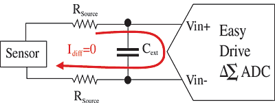 Figure 1. Easy Drive technology automatically cancels differential input current, thus allowing direct digitization of large external RC networks. |
Rather than onchip buffers that can compromise performance, Easy Drive uses an architecture that maintains 0.002% F.S error with input RC networks up to 100 kV and 10 µF. Among the benefits are:
- Rail-to-rail common-mode input range
- Direct digitization of high-impedance sensors
- Elimination of sampling spikes seen at the ADC input pins
- Simple, external low-pass filtering
- Noise and power reduction
- Cancellation of external RC settling errors
- Easy interface to external amplifiers
- Removal of transmission-line effects for remote sensors
Operating Principle
ΣΔ converters combine many low-resolution conversions into one high-resolution result. Most commercially available devices combine hundreds or even thousands of 1-bit conversions into a single 16-, 20-, or 24-bit output, but it is obviously much easier to implement a 1-bit than a 24-bit converter. To achieve high resolution, the input is sampled frequently during the conversion cycle.
The problem is that the input structure of ΣΔ converters is a switched capacitor network. Capacitors are switched at up to 10 MHz between the input, reference, and ground as a function of the final output code. Each time these capacitors are switched to the ADC input, a current pulse is generated. A pattern of charging/discharging pulses is seen at the input pin of the ADC. This pattern is a complex function of the input and reference voltages. External RC networks that do not completely settle during each sample period cause large full-scale errors.
The trick to solving this problem is to take advantage of the oversampling properties of ΣΔ converters. The front-end capacitor switching on a per-sample basis is identical to conventional ΣΔ converter sampling. An innovative front-end sampling architecture controls the switching pattern of the capacitor array. When summed over the entire conversion cycle, the total differential input current is zero, independent of the differential input voltage, common-mode input voltage, reference voltage, or output code. The common-mode input current is constant and proportional to the difference between the input common-mode and the reference common-mode voltages.
RC networks placed upstream of ΣΔ ADCs significantly improve the converters' performance and ease of use, while providing low-pass and anti-alias filtering. External RC networks applied to the input of the LTC2480 simply integrate (average) the input current spikes generated by the ADC. Since the average differential input current is zero, the total error introduced by the external RC network is zero if the resistance tied to the plus/minus inputs to the ADC is balanced. Resistances up to 100 kV, combined with capacitors up to 10 µF may be placed in front of the ADC with <0.002% F.S. error (see Figure 2).
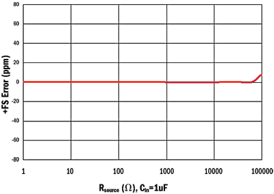 Figure 2. Full-scale errors due to incomplete settling of a large external RC network are automatically removed. |
Conventional ΣΔ converters with the same input network have >10% F.S. errors (100,000 ppm).
Furthermore, no errors are introduced even if the external resistances are not balanced, as long as the common-mode input voltage is equal to that of the reference voltage. Even if the input common-mode voltage is not equal to the reference common-mode voltage, the differential input current remains zero and the common-mode input current results in an offset voltage that can be removed through system calibration.
Bridges, along with RTDs, thermocouples, and other sensors may tie directly to the ADC input without having to add external or onchip amplifiers. The addition of external capacitors reduces the charge kickback spikes seen at the input of the ADC. An external 1 µF capacitor reduces a 1 V spike to 18 µV. This improves the noise performance of systems in which the sensor cannot be placed near the ADC input, and eases the drive requirements in applications where external amplifiers are used. The addition of a large resistor between the amplifier output and the ADC input isolates the amplifier from the large bypass capacitor, thus improving its stability.
Achieving Data Sheet Performance in the Real World
One challenge familiar to designers of high-performance data acquisition systems lies in achieving data sheet-specified perfor -m ance in a real-world environment. An advantage SD-type ADCs offer over the alternatives is onchip digital filtering (noise suppression). The drawback is the drive requirements inherent in ΣΔ ADC architectures. To demonstrate Easy Drive technology's ability to overcome this hurdle, a practical test case was characterized (see Figure 3).
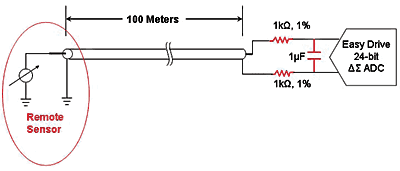 Figure 3. A practical test was devised to demonstrate Easy Drive’s measurement capabilities under real-world conditions. |
Precise measurements of offset, noise, and linearity were measured under extreme test conditions. A remote sensor was digitized through 100 m of cable applied to an RC network with low-accuracy 1% resistors. When a remote sensor voltage was swept from 0 to 20 mV, <1 ppm linearity, noise levels of 650 nVrms, and offsets below 5 µV were observed (see Figure 4 and Figure 5).
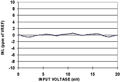 Figure 4. Results of the test setup in Figure 3 indicated <1 ppm linearity. |
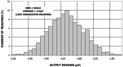 Figure 5. The same test platform results showed noise levels of 650 nVrms and offsets <3.5 µV. |
Solving Some Fundamental Problems
An oversampled ΣΔ ADC directly connected to a long cable and a low-precision RC network can seriously limit system accuracy due to transmission line effects, noise, and DC settling errors. When the sampling network injects high-frequency current into the cable, the resulting voltage spikes are reflected through the long wire and result in excessive noise and reduced accuracy. The way to solve this problem is to place a bypass capacitor across the input to the ADC. The capacitor serves as a charge reservoir for the sampling network and reduces the voltage spikes by the ratio of the internal sampling capacitor to the external bypass capacitor. A 1 µF bypass capacitor reduces the voltage spikes by a factor of 50,000 (1 V spikes are reduced to 18 µV) and achieves the noise and accuracy specified by the manufacturer.
Adding the capacitor also corrects input settling errors. Typical 24-bit high-resolution ΣΔ ADCs sample at time intervals on the order of 10 µS. To fully settle with a 1 µF bypass capacitor, the source impedance must be <1 V; otherwise, the accumulation of charge settling errors over the complete conversion cycle will cause offset and full-scale errors. Easy Drive automatically removes the differential component of this error. The remaining common-mode error is reduced to a fixed offset as a function of the external resistor-matching seen at the ADC's plus/minus inputs. In this extreme case, 1 kV external resistors with 1% matching result in a 3.5 µV offset while the linearity and noise are unaffected.
Another issue is noise rejection. Say a signal path contains a 100 m wire connected to a low-voltage source in a very noisy environment. Line frequency noise is rejected by the onchip digital filter and guaranteed by the high-accuracy onchip oscillator. High-frequency noise is rejected by the external low-pass filter formed by the input bypass capacitor and external resistors.
One historical solution to the input current settling problem is to integrate a buffer amplifier and a ΣΔ ADC on the same chip. This isolates the ADC input from the switched capacitor array, making the converter input appear high impedance. While this looks good on paper, in actuality data converters with onchip buffers and amplifiers have limitations. The common-mode input range can no longer swing rail-to-rail. Input signals must be shifted at least 50 mV above ground and a volt or more below the supply voltage. Amplifier offset errors, offset drift, power supply rejection ratio, common-mode rejection ratio (CMRR), and noise directly combine with the input signal and degrade converter performance. Additionally, onchip amplifiers require significant power to drive the high-speed capacitive sampling network. Most manufacturers of ΣΔ ADCs using this technology therefore offer a mode to shut off and bypass onchip amplifiers.
Another approach is coarse/fine input sampling. During the first half of the sampling period (coarse), the input voltage is sampled through an onchip buffer amplifier, thus isolating the ADC input from the charging capacitor. During the second half of the sampling period (fine), the buffer is switched off and the capacitor is tied directly to the input. Although this technique reduces the spikes seen at the input of the ADC, it also results in nonlinear settling errors as a function of op-amp offset voltage, CMRR, input signal level, and external RC time constants. Manufacturers of ΣΔ ADCs based on this approach generally use bypass course/fine sampling for input signal levels below 100 mV.
Summary
Easy Drive technology simplifies the drive requirements of ΣΔ ADCs. The solution lies in a purely passive input-current cancellation algorithm that enables rail-to-rail inputs without the added power requirements of onchip buffer amplifiers and the errors they introduce. Easy Drive allows the ADCs to directly interface to high-impedance sensors, low-pass filters, and input bypass capacitors without degrading DC performance.
For further information, contact Doug Dickinson, Linear Technology, Milpitas, CA; [email protected].