
Several of the challenges can be solved by carefully selecting the amplifier used to drive the ADC. Today’s ADCs have phenomenal signal-to-noise ratio (SNR) and resolution. By understanding the relationship between amplifier specifications and converter requirements, you can optimize resolution and throughput of the data acquisition system.
Noise Considerations
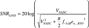
The noise of the amplifier will affect both the SNR and transition noise of the ADC. A simple guideline is to keep the amplifier’s noise at the same level as the ADC’s noise. The signal-to-noise loss expression in Equation 1 expresses the effect of the amplifier’s noise on the ADC’s signal-to-noise ratio (SNR).
 |
(1) |
Where:
VNADC = the rms noise of the ADC in volts
It can be calculated using Equation 2:
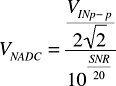 |
(2) |
Where:
VINp-p = maximum input voltage range of the ADC (in volts)
f–3dB = –3 dB bandwidth of the input filter (in Hz)
eN_RTO = equivalent output referred noise of the amplifier (V/rt-Hz)
To calculate eN_RTO, multiply input noise by the noise gain of the op amp. For instrumentation amplifiers, refer to the noise equation in the data sheet.
For example, assume that a unity gain op amp, G=1 with 2 nV/rt-Hz wideband noise, drives an ADC. The ADC has a 90 dB SNR, a 5 Vp-p input voltage, and a 250 kHz bandwidth (limited by the anti-aliasing filter). Using the VNADC equation, the ADC's noise is 56 μV rms and the SNR loss is 0.002 dB.
Settling Time
Another consideration in maintaining the ADC's performance is to use an amplifier that can settle to 1 LSB from a full-scale step within the acquisition time of the converter. This ensures that the full sampling rate of the ADC can be used and that the correct value is converted from analog to digital. If, for example, the amplifier settles to only 90% of its final value by the end of the acquisition window, the converter will convert an erroneous result. This is particularly relevant for data acquisition systems that use a single ADC with multiplexed inputs; the ADC samples each input channel in sequence and the post processor reassembles the data as multiple signals. Since one channel may have a small signal and the adjacent channel may have a large signal, the multiplexer and the amplifier must transition from the small signal to the large one within a conversion cycle. The solution is to select an amplifier (and multiplexer) with settling time less than the acquisition (and conversion) time. Sixteen-bit accuracy requires 0.0015% and 18-bit accuracy requires 0.0004%. While many older amplifiers were specified to 0.01%, newer amplifiers specify settling time to 0.001%.
For applications that require digitization of wide-bandwidth signals, such as vibration analysis, distortion is a critical specification. Successive-approximation ADCs have switched capacitor inputs that exhibit nonlinear input impedance. When the switched capacitor opens, “kickback current” is delivered to the output of the amplifier. The amplifier reacts to the injected charge, resulting in increased total harmonic distortion (THD). An RC filter with a 15 to 50 ohm resistor and a 1 to 2.7 nF capacitor are typically placed between the amplifier and the converter to isolate the amplifier from the ADC’s kickback. This low-pass filter also filters the amplifier’s reaction to the charge injection. Using a resistor that is too small provides insufficient isolation and can destabilize the amplifier. Too large a value causes a voltage drop across the resistor; the signal at the amplifier’s output no longer correlates with the signal at the input of the ADC. The optimal value balances destabilizing the amplifier and maximizing the THD of the ADC.
The ability of the amplifier to swallow the kickback current is related to its output impedance, which is a function of the loop bandwidth. Equation 3 correlates open-loop gain as a function of frequency and the feedback factor.
| (3) |
Where:
a(f) = open loop gain as a function of frequency
β = feedback factor
ro = impedance of the output stage
As the bandwidth increases, the gain of a voltage-feedback amplifier falls at –20 dB/decade. As the gain decreases, the output impedance increases. If THD specifications are important in the application, select an amplifier that has a high gain-bandwidth product. This ensures that linearity errors are divided by a large open-loop gain. It also keeps the amplifier’s output impedance low.
Figures 1 and 2 show the general correlation between gain-bandwidth product and THD. Figure 1 shows a popular op amp with a unity gain bandwidth of 1 MHz. When used with a 16-bit, 750 Ksps successive-approximation ADC, such as Analog Devices’ AD7612, THD is –63 dB.
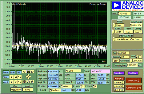 Figure 1. The FFT of the AD7612 when driven by an op amp with a 1 MHz gain-bandwidth product |
In contrast, Figure 2 shows an amp with a 50 MHz gain-bandwidth product.
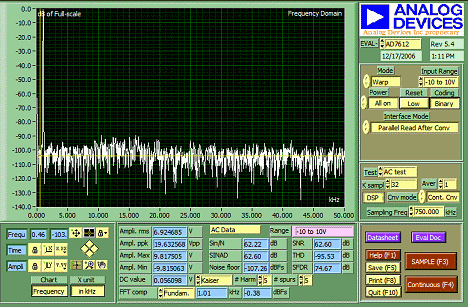 Figure 2. The FFT of the AD7612 when driven by an op amp with a 50 MHz gain-bandwidth product |
The system’s THD is –96 dB. Both are configured in the test circuit shown in Figure 3.
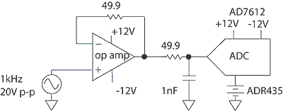 Figure 3. Test circuit for comparing the effect of op amp gain-bandwidth product on an AD7612 |
While amplifier bandwidth is a good indicator of distortion, it is not a definitive one. Some amplifiers, such as Analog Devices’ AD8250, have distortion-cancellation circuitry that makes it possible for a low-distortion THD of –111 dB with 15 MHz of bandwidth, as shown in Figure 4.
 Figure 4. The FFT of the AD7612 when driven by an analog front-end composed of the ADG1209 multiplexer and AD8250 digital programmable gain instrumentation amplifier |
Reducing Differential Measurement Errors
Measurement of small signals—such as those from a thermocouple—is usually made differentially. Common-mode rejection (CMR), a comparison of differential gain to common-mode gain, is the most important criterion for differential measurements. Since many SAR ADCs have CMR of 60 dB or less, it is important to design an analog front-end that can reject common-mode signals. Many topologies offer high CMR; one of the most popular architectures is the three-op-amp instrumentation amplifier (Figure 5).
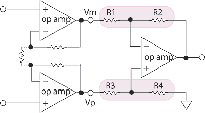 Figure 5. CMR of a three-op-amp instrumentation amplifier is determined by the matching the ratio of R1:R2 to the ratio of R3:R4 |
The three-op-amp in-amp can be built using resistors and op amps or it can be purchased as a monolithic IC. While building an instrumentation amplifier from discrete components offers flexibility and the ability to tailor specifications to the application’s needs, its disadvantages are size, number of components, and design time.
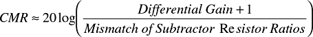
Common-mode error of a three-op-amp in-amp arises from the mismatch between the resistor ratios in the subtractor. When selecting resistors, a typical mistake is to go to great lengths to match the absolute tolerance of the resistors. CMR is at its maximum when the ratio of R1:R2 is matched to the ratio of R3:R4. The following numerical example will illustrate this point. Plug the following resistor values: R1 = 1K; R2 = 2K; R3 = 3K; and R4 = 6K into the subtractor’s transfer function shown in Equation 4.
| (4) |
Where:
Vp = the positive input signal
Vn = the negative input signal
Even though the absolute values of R3 and R4 are considerably different than those of R1 and R2, the output will be 0 V, indicating infinite CMR. In reality, there is always some mismatch but this can be reduced by using resistor arrays with low group mismatch. They tend to be more expensive than stand-alone resistors but offer high CMR. Vishay’s ORN thin film resistor arrays are available in a Z grade that has ±0.01% ratio tolerance. A ±0.01% ratio mismatch has a worst-case mismatch of 0.02%, which translates to a CMR of 80 dB for a gain-of-1 in-amp. An equation for calculating CMR based on resistor ratio mismatch for a traditional three-op-amp in-amp is shown in Equation 5.
 |
(5) |
Monolithic three-op-amp instrumentation amplifiers tout high CMR. Laser trimming techniques are employed to match the ratios, providing instrumentation amplifiers with minimum CMR of 90 dB and higher. Figure 6 shows the schematic of a data acquisition signal chain using a monolithic in-amp.
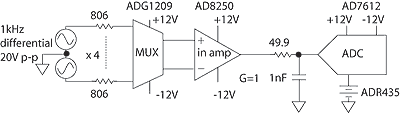 Figure 6. Example of a data acquisition front-end composed of the ADG1209 and the AD8250. The AD7612 can sample ±10 V signals, eliminating the need to attenuate in front of the ADC |
They offer reduced design time and a small footprint but they are harder to tailor to a specific application.
Interfacing to the Real World
Fortunately, not all transducer signals are small. While many thermocouples and bridge-based sensors output small voltages, many integrated transducers output 10 V. Conditioning ±10 V signals enables end users to interface their data acquisition system with numerous legacy instruments. Many of today’s ADCs operate on voltages of 5 V or less, requiring the input signal to be level-shifted and attenuated before it can be digitized by the ADC. The challenge is to do so without degrading the signal.
Attenuation should follow the common-mode rejection stage. In other words it should occur after the instrumentation amplifier and initial signal conditioning. By attenuating after the instrumentation amplifier and before the ADC, both the signal and the noise are attenuated. An op amp in an inverting topology with a gain of 1/4 following the in-amp can serve as an attenuation and ADC driving stage. The noise of the resistors, expressed in the Johnson noise equation (Equation 6), will contribute to the system noise. Reducing the value of the resistors in the feedback of the amplifier will reduce noise. However, a trade-off must be made between the amplifiers' ability to drive a heavy load and reducing the resistors to the smallest possible value.
| (6) |
Where:
k = 1.38 x 10⁻²³J/K, Boltzmann’s constant
T = absolute temperature in degrees Kelvin
R = resistance in ohms
B = bandwidth in Hz
Advances in process technology have enabled some ADCs, such as the AD7612, to sample ±10V signals. The benefit of using such a converter is that it requires fewer amplifiers and resistors, which reduces the number of noise sources and simplifies design.
Details Matter
Designing general-purpose DA systems is an exercise in producing a flexible solution; the wide variety of input sources and applications make optimizing the analog front-end a challenge. Maintaining the performance of the ADC is crucial for accurate digitization. Designers can ensure high SNR and low distortion by reducing the amplifier and resistor noise, the converter’s source impedance, and the amplifier settling time. Differential signal integrity is maintained by matching resistor ratios in the instrumentation amplifier. Ultimately, the objective is to acquire signals from the environment. All of these challenges can be managed by paying attention to key details.
References
1. “AD7612 Data Sheet.” Rev. 0. Analog Devices, 2006.
2. Gerstenhaber, Moshe. Personal Interview. 21 December 2006.
3. Guery, Alain and Kitchin, Charles. “High Speed Op Amp Drives a 16-Bit, 1-MSPS Differential-Input A/D Converter.” Analog Dialogue 36-06. 2002. 1–4
4. Mueck, Michael. Personal Interview. 21 December 2006.
5. Wayne, Scott. “Finding the Needle in the Haystack.” Analog Dialogue 34-1. 2000. 1.