
When conditioning signals for input to ADCs there is usually a compromise between changing the gain of the signal and adding offset to ensure that the signal has the right range and common mode voltage for the ADC. This article will describe how to meet the full dynamic range of an ADC (the sweet spot range) based on a given input signal, while preserving the linearity of the input signals. It also provides a DC-coupled signal as an output, preserving low-frequency response when compared to AC-coupled designs.
Whether a signal needs to be amplified, attenuated, or level-shifted, there is little advantage in using passive components by themselves to perform these functions. Inexpensive amplifiers now offer better accuracy than passive components in level-shifting operations and their combination of gain and level-shifting allows users to meet simultaneous requirements in a given design. The approach uses a standard amplifier circuit that can be represented by two sets of simultaneous equations, which can be solved in a few minutes with a programmed calculator. This design also has the advantage of mapping bipolar input signals to a single-supply ADC without requiring transformers or charge pumps to create a negative rail.
The inverting amplifier circuit shown in Figure 1 includes a voltage reference to provide offset for a bipolar input signal of ±4 V, which is being conditioned for a single-supply ADC with a 2.5 V reference. The transfer function of the circuit is given in Equation 1:
| (1) |
where:
| Vout | = | Output voltage of amplifier |
| R1 | = | Inverting resistor |
| R2 | = | Input resistor |
| Vref | = | Reference voltage |
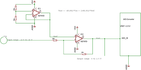 Figure 1. An inverting amplifier circuit with gain and offset (Click image for larger version) Figure 1. An inverting amplifier circuit with gain and offset (Click image for larger version) |
The circuit in Figure 1 attenuates and level-shifts the signal to match the 2.5 V reference of the ADC. The input resistor R2 should always be chosen first to match the signal source impedance for good voltage transfer. Many designers will be tempted to use a voltage divider before the input resistor R2 to attenuate the input signal. However, there are consequences to this approach: A resistor-divider can compete with the input impedance R2, which can change the gain characteristics of the amplifier; and a resistor-divider with low input impedance can draw excessive current and will unnecessarily load the signal source. The amplifier-reference circuit in Figure 1 avoids these compromises and provides the option of high-input impedance for the signal source (by choosing a larger R2) and allowing the combination of the reference and gain resistors to reduce the input signal amplitude without overloading it.
Due to the nature of the inverting amplifier in Figure 1, a –4 V input will correspond to a 2.5 V output and a 4 V input will correspond to a 0 V output. These two constraints can be expressed as two equations of the form of Equation 1 as shown below in Equation 2:
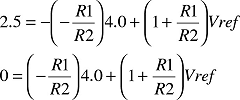 | (2) |
These two equations are solved simultaneously for the two variables, the ratio R1/R2 and Vref. In this example, R1/R2 = 0.313 and Vref = 0.953 V.
Using these solutions, the design will meet the input-to-output criteria shown in Figure 1 without requiring a negative supply to handle the –4 V input. An additional advantage is that not only do the input extremes of –4 V to 4 V match the output extremes of 0–2.5 V, but the transfer function is linear in between these points as Equation 1 shows. Choosing R3 and R4 within the accuracy required allows the realization of the reference voltage Vref. A precision reference can also be substituted for this circuit if desired.
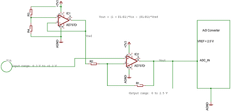 Figure 2. A noninverting amplifier circuit with gain and offset (Click image for larger version) Figure 2. A noninverting amplifier circuit with gain and offset (Click image for larger version) |
A similar design, shown in Figure 2, uses a noninverting gain. This provides high input impedance due to the noninverting input of the op-amp. Because the input signal is connected directly to the amplifier it must be within the rails of the amplifier. Under these circumstances it is still possible to meet output requirements based on inputs using the noninverting gain formula in Equation 3:
| (3) |
If, for a given example as shown in Figure 2, we wish to translate a signal input range of 0.3–1.2 V over the range of the ADC's input (0–2.5 V), we can establish these requirements using Equation 3 as follows in Equation 4:
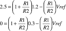 | (4) |
The solution is R1/R2 = 1.78 and Vref = 0.47 V.
This shows that the noninverting amplifier configuration can translate the input signal range (within the limits of the amplifier rails) to the desired output range. Vref is then chosen by adjusting R3 and R4 to meet the requirements.
In conclusion, the method shown for meeting the ADC sweet spot balances the dynamic range of input and output requirements without compromising signal integrity or bandwidth.