
 |
After a lingering fallout period the MEMS-based sensor industry is now back on a reasonable growth track, with significant advances and manufacturability improvement in MEMS-based products outside the proven sectors. Sensing and actuation for industrial and biomedical applications in particular hold major promise. But whether these efforts come to fruition depends on several key factors, one of the most important of which is foundry business model and cost.
Foundries: What Went Wrong?
Looking back at the past few years of foundry experience, were the shutdowns the result of economic changes and cash shortages throughout the supply chain? While admittedly money was tight and coming from the top down, fabless developers were optimistic. Many of them did indeed secure interest and commitments from potential customers. So what went wrong? While in some cases the designs (especially in the telecom sector) were far too complex to be reliable given manufacturing capability of the time, the failed foundries had a few traits in common.
They tried to appeal to a broad base of developers. As MEMS engineers are aware, MEMS devices can depend on a wide range of processes, with an enormous number of variables. The devices that were already on the market had been commercialized only after years of process refinement and test. R&D teams typically need extensive amounts of time to reach conclusions about the physics of the processes and materials, and the causes of failure. Tests demonstrate that even one device manufactured using a single material such as polysilicon may require marked variations in process, depending on the source of the polysilicon and the deposition method.
The failed commercial foundries tried to address multiple product opportunities across multiple markets and multiple processes, with the result that their R&D time and even prototype manufacturing variables increased exponentially. For smaller foundries, this was the kiss of death.
They lacked experience with high volumes and cost-cutting methods. The operators of these independent foundries, many of whom began in academic R&D, had little experience with high-volume production and cost-cutting expertise necessary for typical infrastructure and optimizations required for mass manufacture. The prevailing attitudes were based on "find a process and they will come," with little regard for how components would fit into existing designs and what the customer was willing to pay.
In the case of RF MEMS, some large-volume consumer equipment manufacturers were seeking MEMS-based components at a price range of $0.10 in volumes of 10 million or more. This figure was to include packaging and test! Clearly, the requirements were beyond the range of smaller fabs, dooming the broad-based business model.
A New Foundry Business Model
In assessing the independent foundries that survived, we can begin to see the formation of a foundry business model that may predominate—at least until the industry can lay a stronger foundation with standard material definitions and some form of semi-standard processes. In particular, while the remaining designers and manufacturers have learned their lesson and have made strides in design for manufacturability and reliability, these qualities alone are no longer enough to persuade volume OEMs to make what is perceived as a frightening jump into replacement technology, even for simple discrete components.
These integrators do, of course, perceive the benefit of the technology and are intent on offering their customers significant value. The question is not if, since MEMS is an increasingly proven technology, but when. Yet, since 2000 these mainstream equipment suppliers—many of whom are virtually giving away technology such as standard cell phones—have become accustomed to squeezing their component suppliers to a bare minimum to realize better margins.
Given such stringent requirements, independent foundries have a crucial role in making innovative MEMS products technically and financially attractive to the mainstream market. This role, while not easy, is a natural fit for foundries, since batch-produced MEMS can facilitate size reduction and cost savings at the same time. Achieving size and unit cost goals in a timely and cost-effective manner, however, is a solution that not all foundries can offer.
The First Step. Fabs must have a few robust, established processes that they know inside and out, through experience and solid statistical process control (see Figure 1). While the drawback is that this may mean some specialization in particular kinds of devices, the major benefit is that these processes provide a baseline starting point.
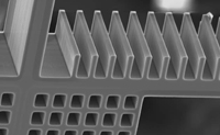 Figure 1.This very precise test structure was created using the latest generation of DRIE equipment. |
Having such proven processes means that foundries know their cost bases in terms of materials, tools and personnel, and that they can offer a certain amount of consistency that shortens time to market. These teams know the properties of materials and base techniques. They are familiar with deposition methods, grain size, how the materials will respond to introduction of other materials, and the factors that may cause structural stress, fatigue, or other failure modes within the typical process parameters.
The Second Step. Established independent foundries must have expert staff and equipment operators on hand whose combined knowledge base can add significant value in reduction of device cost, size, and power consumption (see Figure 2). In some cases the fab will have its own design-for-manufacture team, and in all cases the facility should offer some form of continuous improvement through total quality management. Silicon Microstructures, Inc., for example, was able to shrink a standard MEMS-based pressure sensor die from 2 x 2 mm to 0.65 x 0.65 mm, to fit more than 25,000 die in a single 6-in. wafer, resulting in major cost reductions to the customer. Similarly, an in-house design team was able to integrate a pressure sensor and DSP on the same small die for a high-performance device aimed at the automotive and medical markets.
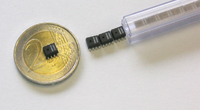 Figure 2. The expert staff at a good foundry will add significant value through size and cost reduction, and continuous improvement processes. Shown here are the smallest available MEMS-based pressure sensors, produced in quantities of 25,000 on a single 6-in. inch wafer. |
Such diverse and experienced teams can offer major insights into improvement methods, from ways to customize equipment for better etch results, to cheaper alternatives in wafer-level bonding for hermeticity.
The Third Step. A good independent foundry will have invested in the needed infrastructure for cost reduction (see Figure 3). Obvious examples include 6-in. wafer cassette handling, which is now the minimum standard for achieving higher volumes in MEMS. The latest equipment can also offer a significant advantage once the team has gained familiarity with it. Stepper technology, track handling, and advanced etching control provide improved MEMS device tolerances at lower cost while also enabling more complex geometries. The newest deep reactive ion etching (DRIE) tools offer unparalleled vertical depth etching and smooth sidewalls for consistent enhanced performance of devices.
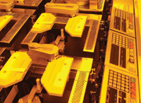 Figure 3. As part of a good equipment infrastructure, a 6-in. wafer line can help reduce costs for foundry customers. |
The Fourth Step. A superior foundry, over years of production of related devices, will typically have developed its own value-added intellectual property (IP) that could significantly enhance a customer's device. Such IP may include integration of additional passive components for greater space savings to combining MEMS devices with improved microelectronics for faster and more accurate performance. The design services team can assist the fabless developer in assessing affordable and reliable options for volume production.
The Fifth Step. A good foundry will move sensor products toward existing semiconductor packaging standards, making it easier for customers to design-in new advanced sensor components and incorporate them into circuitry with automated pick-and-place equipment. The smallest available pressure sensors have already arrived at this point, where they are housed in JEDEC-conformable SOIC-8 packages and are circuit board ready for any manufacturing facility.
Summary
The opportunities for MEMS are wide open and the technology is established. While there are no one-size-fits-all foundry solutions, customers who require high-volume manufacturing capability can take their pick from an assortment of competing facilities.
The key lies in finding a partner with the knowledge, experience, and up-to-date infrastructure that can help get the product to market at the necessary cost point that will appeal to major OEMs, while ensuring manufacturability and quality.
Jim Knutti, B.S., M.S., Ph.D., can be reached at Silicon Microstructures, Inc., Milpitas, CA; 408-577-0100, jim.knutti @si-micro.com, www.si-micro.com
;