
Onboard automotive sensing systems have increased in variety and usefulness in the past decade. They are most frequently offered as options on premium-priced automobiles, often from European manufacturers. There are ultrasonic sensors to measure distances in maneuvers such as parallel parking and also video systems for night vision. The various sensing systems can be classified as safety enhancers, convenience items, or a combination of the two.
Automotive radar has also been available, as with the other sensor types, chiefly on high-end vehicles. It can have high safety value because of its sensitivity in detecting and locating other vehicles, especially at highway speeds, and is referred to as long-range radar because it looks for obstacles that are 200–300 m ahead. Long-range radar has been combined with the vehicle's cruise control to create what is known as Adaptive Cruise Control.
Here's how it works: Suppose you are driving at 80 mph in the fast lane on an interstate highway and you're using cruise control. The car ahead of you, also in the fast lane, going at a speed of only 75 mph. The long-range radar will spot the car, note its location and speed, and communicate with your cruise control to lower your speed to 75 mph and to keep a safe distance between the two cars. If the car ahead speeds up to 80 mph or more, or if it moves to the right, Adaptive Cruise Control will boost your speed back up to 80 mph. At any speed, however, long-range radar can work to maintain a safe distance between your vehicle and the vehicle ahead and thus avoid rear-end collisions.
Because of long-range automotive radar's high safety value, it would be beneficial to extend its use beyond high-end cars to the less expensive models. Unfortunately, it is inherently costly to acquire and assemble the components needed to make an automotive radar system.
A few years ago the Fraunhofer Institute IZM, Germany's research center whose many divisions turn feasible concepts into manufacturable realities, saw a way to reduce the cost of these systems. Automotive radar systems typically consist of components attached to a printed circuit board (PCB). The researchers at Fraunhofer foresaw that costs could be reduced by using an assembly method that places the components inside the PCB. The German government then funded a consortium involving, among others: Bosch, the automotive parts manufacturer, Wuerth Elektronik, makers of PCBs, and the Fraunhofer Institute.
The benefits of moderate-cost, long-range automotive radar would extend far beyond the protection of the driver and passengers in a top-end BMW that is cruising the autobahn at high speeds. On a more mundane level, most of the truck accidents in Germany are rear-end collisions—caused when the truck driver couldn't quite stop in time—that take place at speeds from 10 to 30 km/h. The vast majority of these accidents could be prevented if Germany mandated the use of long-range radar on all trucks. Such legislation does not exist today, but substantially decreasing the cost of long-range radar systems would make the idea more attractive. Today, for example, BMW charges about 1800 € for Adaptive Cruise Control with stop-and-go capability. Therefore, a primary goal of the consortium was to reduce the cost of manufacturing for a long-range radar system by about 30% to make the technology feasible for integration in mid-priced autos.
Streamlined Assembly
Electronic systems installed in automobiles have generally undergone more rigorous development than systems destined for most other applications. The automotive environment subjects electronics to drastic temperature fluctuations, noxious fumes, and endless shock and vibration. Under normal circumstances, lopping a small percent off the cost of manufacturing a PCB populated with integrated circuits, resistors, capacitors, connectors, and all the rest would be a significant challenge.
We can understand part of the cost if we consider the steps involved in applying a plastic-encapsulated microcircuit (computer chip) to a PCB. The chip is removed from the plastic tube or tape that it was supplied on, is picked up by a vacuum or tweezers, and placed on the solder paste on the PCB. Later, the whole board is heated to around 260°C to melt the solder so that the metal leads sticking out of the microcircuit can make electrical connections with the board. After cooling, the board is cleaned and tested. Many handling steps are involved, presenting many opportunities for damage to the plastic-encapsulated microcircuit.
The Fraunhofer Institute had a big advantage in modifying this scenario. Its Chip in Polymer technology has the same basic purpose as the solder-reflow process described above—to connect the silicon chip with display units, controls, and other parts of the system of which the chip is a part. The approach, however, is very different.
Chip in Polymer
Chip in Polymer begins with a very thin substrate—much thinner than the typical PCB. The substrate may be FR4 (a glass-reinforced epoxy laminate) or copper. The item to be embedded is typically a silicon chip. The silicon chip, previously thinned to a thickness of approximately 50 µm, is adhesively bonded face up onto this substrate. Then a layer of resin-coated copper is placed on top. The resin conforms to the height of the chip so that the copper layer on top remains flat.
When the resin has cured, a laser drills holes down through the copper-resin to the contact pads on the chip. The holes are plated with copper, and the copper layer on top is etched in a pattern that leaves only the copper traces that will connect the chip to the rest of the system (Figure 1).
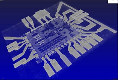 Figure 1. X-ray CT image of embedded VCO (Voltage Controlled Oscillator) chips connected via two metal layers |
The Fraunhofer team used the Chip in Polymer approach along with a second method called Duromer Embedding. In this method, the chip is first attached face down onto a carrier tape. The tape and chip are placed in a transfer-molding tool, where the chip is overmolded by transfer molding. The thickness of the mold compound over the chip backside can be controlled so that all chip-mold compound combinations have the same thickness, no matter what the thickness of the silicon. To assemble the 77 GHz radar system, all of the individual radar ICs were embedded by the Duromer process into one molded module (Figure 2), and Chip in Polymer was then used to attach this 1 mm thick module to the core substrate.
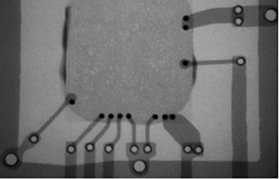 Figure 2. X-ray image of embedded SiGe chip |
The radar chip itself is a 1.8 by 1.7 mm silicon germanium (SiGe) 77 GHz voltage control oscillator (VCO) that runs off a 5.5 V supply voltage and has an operating temperature range of –40°C to 125°C. The VCO replaces the Gunn oscillator; both devices can be tuned to oscillate between 70 and 80 GHz, but the Gunn oscillator is hundreds of times larger than the chip. When a diode, such as those on the VCO, is biased, the usual result is an upward curve into a positive resistance area. The SiGe chip, in contrast, goes through an S curve, alternating between negative resistance (the downward part of the curve) and the upward positive resistance. This alternation into the negative region is what causes the oscillation and launches the radar signals.
By removing several process steps and by doing without wires, wire-bonding, and solder, Fraunhofer researchers lowered the cost of the whole radar assembly by the desired 30%. Because the radar ICs are all embedded at the same level, it was possible to use the antenna arrays within the IC to employ a narrower radar beam. A wide radar beam has a lower spatial resolution; it can tell how far away an obstacle is, but it cannot reliably determine the obstacle's left-to-right position. To make a narrower beam requires the development of new algorithms, which were written by researchers at the university in Stuttgart; the corresponding antenna array layout was designed by university scholars at Erlangen. The resulting narrow-beam radar sweeps back and forth and does a better job of locating an object and of judging the object's dimensions to distinguish, for example, between a car and a motorcycle.
Installation on the Horizon
The completed module with its embedded radar ICs (Figure 3) passed the electrical and longevity tests that are standard at the conclusion of development. One test, though, was unnecessary—the shock and vibration tests that are often carried out on electronic assemblies destined for harsh applications. Earlier work during the Chip in Polymer development program had already shown that the chips were so well protected that further testing was unnecessary. The embedding and material-matching necessary to create this type of assembly ensures minimal movement of parts relative to one another during vibration or mechanical shock and ensures minimal differential stress under large temperature excursions.
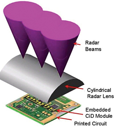 Figure 3. The completed automotive radar module |
The embedded-chip radar system is not being installed in new vehicles just yet, primarily because the incorporation of new safety equipment in general proceeds slowly. However, expect to see the first versions in two to three years.
ABOUT THE AUTHOR
Tom Adams, BA, MA, can be reached at [email protected].