
A widening range of complex designs—such as automated test equipment (ATE), medical instrumentation and monitoring devices, data acquisition (DA) systems, laboratory instruments, and programmable logic controllers (PLCs) for industrial automation—depend on high-resolution ADCs to link the "real world" of analog phenomena and the "processing world" that uses digital information.
The fundamental requirements for ADCs revolve around resolution, accuracy, and bandwidth; other important considerations are signal-to-noise performance, distortion, and latency. Some applications need rapid responsiveness to process high-frequency or continuous readings from sensors. For others, the ability to multiplex multiple signals within the ADC is important, e.g., for PLCs that can simultaneously monitor and integrate real-time inputs from multiple sensors.
The cost of the device and the cost of any required support circuitry are also important considerations for component selection. This is particularly true with ADCs, especially when used in a high-performance multiplexed environment, because the required support circuitry can vary significantly depending on the type of ADC selected.
The Traditional SAR Approach
Traditionally, the types of high-performance applications mentioned earlier have been designed around successive approximation register (SAR) ADCs, which provide a series of "snapshots" of the data at successive points in time. SAR ADCs generally have been targeted toward applications that require fast response and low latency. However, because they are sensitive to noise and have relatively low differential nonlinearity (DNL) performance, they often need significant support circuitry, driving up the overall cost and complexity of the design.
Poor linearity cannot be averaged out by oversampling the signal. To compensate, design engineers must overspecify the ADC and overdesign the system. Similarly, in inherently noisy environments, the SAR ADC's higher noise sensitivity and limited noise-rejection capabilities present additional design challenges, for instance, when they are used in PLCs on production floors or clusters of multichannel ATE systems in close proximity.
In contrast, ΔΣ ADCs have traditionally delivered superior DNL and noise performance while requiring less-complex support circuitry. However, they have not been considered appropriate for use in high-performance applications requiring low latency and high conversion rates, to achieve wide signal bandwidth.
A New Architecture
The CS556x/7x/8x family (see sidebar "The CS556x/7x/8x Family") of high-throughput ADCs from Cirrus Logic consists of 16- and 24-bit devices, built around an advanced high-throughput ΔΣ architecture designed to fully settle on every conversion at rates up to 200 Ksps. This provides high-response, low-latency performance comparable to or better than SAR ADCs and allows them to function as cost-effective alternatives in those applications that traditionally required SAR ADCs.
Single-Cycle Latency
In the past, ΔΣ ADCs have focused primarily on the highest resolution measurement of slow-changing signals such as those from temperature sensors and weigh scale load cells. Since noise rejection is critical to obtaining measurement accuracy in noisy digital environments, designers have become accustomed to seeing long "sinc"-type digital filters that reject line frequency interference, such as 50 and 60 Hz line frequencies and their harmonics. The filters are easy to implement, consume minimal die area, and feature excellent noise performance. However, such filters tend to require a large number of conversion cycles to process the input signal before delivering an output word and thus are slow to respond to a change in the input. For example, the left side of Figure 1 illustrates the 3-conversion latency of the digital filter used in the CS553x family of high-resolution ADCs.
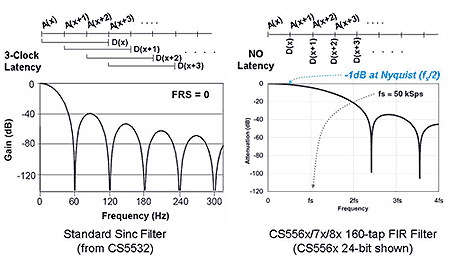 Figure 1. CS556x/7x/8x ADC flat FIR filter: SAR performance from a ΔΣ ADC |
The CS556x/7x/8x family incorporates a fast FIR-type filter that offers two major advantages. First, the filter is nearly flat to twice the sampling frequency, providing users with unrestricted frequency response. Second, (as shown on the right side of Figure 1) the filter is processed quickly, and delivers a new output word at the end of the sampling cycle. This single-conversion latency allows the new devices to offer the noise and DNL performance of a ΔΣ ADC with the high sample rate and Nyquist bandwidth of a SAR converter.
The new design also overcomes the "quiet period" imposed by many conventional SAR devices, in which the ADC output cannot be accessed during certain parts of the sampling process. Testing of these new ΔΣ devices has demonstrated that accessing the digital outputs, at any time during the conversion cycle, has no impact on the performance of the device, including during full-speed operation.
Conversion on-demand (another SAR feature) makes these devices ideal for conducting asynchronous measurements, which are often required in production environments. This allows the designer to coordinate conversions with specific events, such as synchronizing flow with pulses or other sensor inputs. In addition, true bipolar inputs, available when running bipolar supplies, avoid the additional gain and offset errors caused by single-supply devices, which require a level-shifter to move a bipolar signal up above ground.
The Advantages of Buffered Inputs
SAR-type converters present numerous design challenges and nowhere is this more apparent than at the analog signal inputs, where the designer must pay attention to component selection and circuit layout to obtain the specified measurement accuracy in the face of multiple noise sources. Considering that the SAR converter itself can be a major noise generator due its high-speed comparator and the fast-changing digital circuitry within the device, this is no small feat.
In comparison, ΔΣ converters offer low sensitivity to noise in addition to their superior accuracy. These new devices provide integrated high-impedance input buffer amplifiers, which make it easy to achieve the full specified performance without complex external input buffer circuits. SAR-based devices usually use some type of sample-and-hold-type circuit to maintain a stable representation of the sampled input signal during the conversion. As a result, the inputs usually present a very low impedance to the signal source. The source usually includes a very large capacitance, requiring a robust amplifier circuit to maintain a stable level at the ADC's input during the dynamic sampling period. In many cases this requires buffer circuits that exceed the cost and complexity of the remainder of the converter circuit; the noise, which is allowed to degrade the sampled input signal, directly affects the accuracy of the conversion. In some applications, this new family of high-throughput ΔΣ-based devices can (in some cases) be driven directly from the sensor, without requiring the buffer amplifiers used by conventional SARs.
Because they oversample at the input, (160 samples/conversion in the case of the 24-bit CS5560/1 devices, with samples taken at an 8 MHz rate), the low-pass filter within the ΔΣ modulator loop and the mathematical averaging performed within the digital filter rejects or ignores much of the noise which creates such problems for SAR-based designs.
Another limitation encountered in the current mixed-signal environment is single-supply operation. The CS556x/7x/8x family offers true bipolar analog input
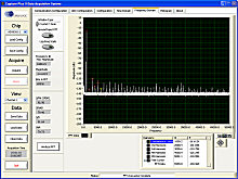 Figure 2. SAR FFT distortion at –12 dB of F.S. (Click image for larger version) Figure 2. SAR FFT distortion at –12 dB of F.S. (Click image for larger version) |
The following sections provide detailed performance comparisons for critical parameters, such as distortion performance and dynamic nonlinearity.
Distortion and DNL
Figures 2 and 3 show a comparison of the distortion performance for a widely used SAR device and the high-throughput ΔΣ CS5571. At
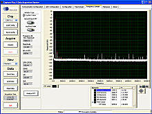 Figure 3. CS5571 FFT noise distortion at –12 dB of F.S. (Click image for larger version) Figure 3. CS5571 FFT noise distortion at –12 dB of F.S. (Click image for larger version) |
Differential nonlinearity (DNL) is basically the measure of code-width variation, normalized to full scale. It is the deviation from a uniform or mean code size, which results in one code size representing a different voltage step size than another code. DNL plots, such as those in Figures 4 and 5, provide a visual representation of variations in code size, which contribute to missing codes, gain, and offset errors. The SAR DNL plot, measured from a competitor's leading SAR device, shows a wide variation in code size, while the accompanying CS5571 DNL plot shows significantly lower error across the entire input range while running at the same conversion speed.
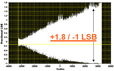 Figure 4. 16-bit SAR DNL plot (in fraction of LSB) |
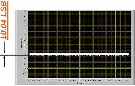 Figure 5. 16-bit CS5571 DNL Plot (in fraction of LSB) |
Typical Application Scenarios
This combination of high resolution and unrestricted signal bandwidth allows designers to perform noise processing and filtering of signals that are tailored to their specific application requirements. Where applicable, this could even include adaptive filtering, in which a system can dynamically modify its filters to adapt to a changing environment.
One of the most exciting application areas is the design of embedded capabilities for PLCs and process control systems. Industrial automation environments have been moving toward decentralized control, using compact, multifunction systems that can be adapted to handle a variety of real-time sensor inputs and provide embedded intelligence and closed-loop responsiveness for implementing local decision loops. High-throughput ΔΣ ADCs allow PLC designers to build in high resolution and low latency while maintaining high measurement accuracy with a consistent level of DNL performance. Real-time closed-loop applications require "no missing code" performance and must avoid steps in the transfer function of the ADC that could result in undefined conditions in the control loop.
Automated test equipment (ATE) requires real-time monitoring and processing of multiple simultaneous input streams. Here again, consistent DNL performance is important for achieving accurate test results, especially when continuously monitoring test information over an extended period of time and watching for small and sometimes subtle signal variations. For those ATE systems used to test and measure noise-sensitive devices, the inherent noise sensitivity of SAR ADCs could interfere with the test results. Designers often use SAR-type converters with significantly higher resolution or speed than required and average multiple samples to get the desired system measurement accuracy. The new family of high-throughput ΔΣ converters can deliver full accuracy with every reading, removing the need for excessive resolution or sampling rates and the need to postprocess less-than-optimal results. The higher throughput equates with lower ATE test costs for the end customer. ATE applications can also benefit from adaptive filtering by allowing the test parameters to be dynamically adjusted during the testing process.
In the field of medical instrumentation, devices such as bedside monitors, blood analyzers, and other diagnostic systems have traditionally used 12- to 16-bit ADCs. Transitioning to higher-resolution ADCs enables designers to digitize a transducer signal directly, without preamplification, and then to perform signal gain and offset corrections in software, improving both accuracy and analytic flexibility.
Weigh scales require highly accurate continuous measurements and are vital for implementing precision batch control and high-speed weighing functions. The actual production output can range from heavy bulk products, such as concrete, to consumer products such as potato chips; however, the need for accuracy and fast response is critical to achieve quality and throughput goals. For example, the weigh scales used in processing bags of potato chips must be able to provide weighing accuracy to 0.01 oz. at high sustained processing speeds.
New Options
Each member of the new family of high-throughput data converters features unprecedented DNL performance, providing designers with a broader range of choices. In fact, since the 16-bit members of this family deliver excellent linearity and noise performance, users can in many cases use a lower-speed ADC and one that provides fully accurate noise-free readings with every conversion.
The data converter architecture addresses the fundamental objectives of high resolution, low latency, and high sample rate. Support for applications with continuous sampling requirements can be provided without necessitating large input buffers and complex support circuitry or imposing undue restrictions on accessing the devices' output buffer.
| The CS556x/7x/8x Family All members of the Cirrus Logic's new family of ΔΣ ADCs incorporate the following key features:
CS5560 Datasheet CS5571 Datasheet Cirrus Logic, Cirrus, and the Cirrus Logic logo designs are trademarks of Cirrus Logic Inc. |