
The operational sensor or actuator in a MEMS device is housed in a cavity between two bonded wafers. The target of acoustic imaging is to check the bond quality of the seal around the cavity because the cavity must be hermetically sealed at all times. The bonds surrounding cavities in MEMS devices must be solid and free from defects that could cause leakage from the cavity or a pressure change within the cavity, either of which would cause the MEMS device to fail in its role as a sensor or actuator.
Less-than-perfect bonds can be the result of process problems, including contamination of one of the bond surfaces; the presence of microparticles between the two silicon wafers; and air bubbles (voids) in the glass frit or other adhesive used to bond the wafers. Poor bonding could also be the result of a flawed layout for applying the adhesive.
It is difficult to consistently and completely exclude the conditions or events that can cause incomplete bonding, in part because the process changes responsible for poor bonding can be extremely subtle. It can also be difficult to identify poor bonding after fabrication because the various types of defect mechanisms tend to create defects that are very tiny or very thin, and thus hard to find via standard methods such as X-ray, destructive physical analysis, and infrared imaging, which can be used if the wafers are not strongly doped and if there is no intervening circuitry.
Such gaps are much easier to image and analyze with acoustic microscopes that use very-high-frequency (VHF, 10–100 MHz) or ultra-high-frequency (UHF, 100–500 MHz) ultrasound, such as that used in Sonoscan C-SAM acoustic microscopes, which are typically used to inspect MEMS wafers after bonding, and sometimes after dicing. In an acoustic microscope, an ultrasonic transducer raster-scans the surface of the sample, pulsing ultrasound into the surface several thousand times a second and receiving the return echoes a few microseconds later. Silicon transmits ultrasound at high speed and with little attenuation, allowing the use of high-spatial-resolution UHF transducers with frequencies such as 230 MHz.
If the two wafers are direct-bonded silicon, there will be no echo at the depth of interest (the location of the wafer-wafer bond) because there is no interface between two different materials (Figure 1). In the acoustic image, the pixel for this coordinate will be black, indicating zero amplitude. But if a silicon wafer and a glass wafer are bonded using an adhesive such as glass frit or a eutectic layer, there will be two echoes: one where the silicon meets the adhesive and one where the adhesive layer meets the glass. In this case, both pixels will be some shade of gray because interfaces between two different solid materials reflect some portion of the ultrasound (perhaps 30% or 50%) and transmit the rest. The precise percentage reflection can be calculated from the material properties of the two materials.
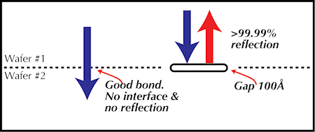 Figure 1. When the ultrasound pulsed by an acoustic microscope meets a good silicon-silicon bond there is no material interface and no echo but a gap as thin as 100 Å reflects nearly all the ultrasound |
A gap at the interface, however, stops the pulse in its tracks and reflects almost all of it back to the transducer. The silicon or glass wafer and the air in the gap have such different material properties that >99.99% of the ultrasound signal is reflected back to the transducer. The pixel from this X,Y coordinate will be white because reflections from gaps have the highest possible amplitude. The completed acoustic image of a bonded MEMS wafer pair will typically consist of millions of black, white, and gray pixels.
The vertical dimension of a disbond or other gap has essentially no effect on its reflectivity because virtually all of the ultrasound is reflected at the top of the gap by the silicon-air interface. Gaps with a thickness down to a small fraction of a micron, and perhaps even less, reflect >99.99% of the applied ultrasound pulse.
The enlarged acoustic image in Figure 2 is made at 230 MHz with an automated C-SAM inspection tool and shows a small area of a bonded MEMS wafer containing a group of four MEMS devices. The four light gray rectangular areas are the wafer cavities. Because the structures within the cavity are not in contact with the wafer through which ultrasound has been pulsed, the cavities themselves appear as large, regular gap features. The arrows point out areas where bonding has not occurred in the seals of three of the four devices. The defect on the right appears to be a complete breach, while the two on the left are, at the moment, only partial breaches that may not yet have compromised the hermeticity of the die cavity. One of the reliability challenges in MEMS devices is that partial breaches or other small anomalies in the seal around the cavities may change and grow as the MEMS device is handled, mounted, or subject to reflow soldering. Ultimately, the cavity's hermeticity may be lost and the device may fail unexpectedly.
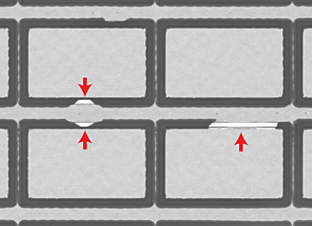 Figure 2. Acoustic image of four MEMS devices in a wafer. White areas are defects in the seals around the cavities |
The Semiconductor Equipment and Materials International (SEMI) global trade association has recently adopted the MS8 standard that provides guidelines for evaluating the hermeticity of MEMS packages, including seal thickness and width, and that recommends the use of acoustic microscopy for evaluating seal integrity. An additional standard, to be issued soon, will deal with measuring the permeability of the seal material to gases and other substances.
The image in Figure 3 shows portions of the seals of two adjacent devices in a bonded wafer pair. The seals in this case contain only small defects, which may be voids or nonbonds. It may be difficult to judge whether defects of this size can cause eventual device failure, but they do point to a processing problem that needs to be identified and corrected.
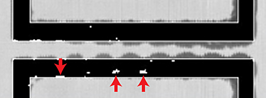 Figure 3. Small defects in the seals around two adjacent wafers |
One of the advantages that Sonoscan brings to acoustic imaging is that automated software can identify–at the wafer level–individual MEMS devices that fail the user's acceptance criteria. The software communicates with the user's Factory Information System software so that later, good MEMS devices can be picked from the carrier tape, while the rejects are disposed of.
Figure 4 is the 230 MHz C-SAM acoustic image of a small portion of a bonded wafer pair. The wide black lines are the seal, made wide to make dicing of the wafer a bit easier. Also visible are numerous features within the cavity, which appear either black or gray. Scattered but widespread lack of bonding is obvious in many locations here. The seal at left has numerous bright areas that indicate lack of bonding between the two wafers. Some of these bright areas form a continuous or nearly continuous pathway through the seal material. After dicing, these areas would become more likely to destroy the hermeticity of the cavity. The same lack of bonding is visible over many of the features within the cavity. It is fairly common to make acoustic images such as this during the early stages of MEMS product development, when process parameters are still being defined and anomalies may be numerous.
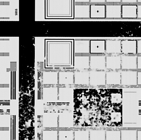 Figure 4. Scattered irregular white areas show lack of bonding between these two wafers |
The acoustic image of a wafer pair of similar devices (Figure 5) shows a very different type of defect. Here, an arrow points out a single tiny particle, probably of silicon, that became lodged between the two wafers, separating the wafers and preventing proper bonding over a roughly circular area (outlined by the red circle) whose size is determined by the height of the particle. In this case, the area of separation crosses the seal zone and encompasses two devices, both of which would lose their hermeticity and would therefore be rejects. Bonding in other areas, including the features within the cavities, has no defects.
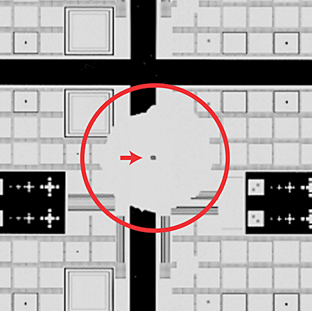 Figure 5. A large, circular disbond caused by a wayward particle (identified with a red arrow) |
C-SAM acoustic imaging can also be used to examine features such as an etched beam. A C-SAM module is used to make a sequence of images at successive depths. For example, 20 images, each of which is taken at a depth 50 µm deeper than the previous image, results in a 20-step slideshow of a 1 mm thick sample. The ultrasound is said to be gated on each 50 µm depth. In a MEMS device, a sequence of thinly gated images is made of the wafer from which the beam originates; these images will show the profile of the beam at each depth. The C-SAM system is also used to image single wafers before they are bonded. The purpose is to locate cracks in the wafers that, like other defects, are hard to find by other methods and use this information to exclude the use of such faulty wafers. While it is easiest to image bonded wafer pairs before dicing, individual MEMS devices are often inspected acoustically after dicing to check for damage that may have been caused by the dicing process or by handling after dicing.
The long-term reliability of the sensors and actuators in MEMS devices depends on the physical integrity of the device. Because acoustic micro-imaging systems are nondestructive, highly sensitive to material interfaces, and can be used to show vertical sequences, they play a large part in achieving MEMS reliability.
ABOUT THE AUTHOR
Tom Adams is a consultant for Sonoscan Inc., Elk Grove Village, IL. For more information, contact Sonoscan Inc., Automated Inspection Division at 847-437-6400 or [email protected].