
Shortly before its quarterly earnings announcement Thursday, Intel promoted its traction with its foundry business, including a collaboration with United Microelectronics of Taiwan on development of a 12-nanometer process platform to be fabricated in Arizona.
On Wednesday, Intel separately announced the opening of its Fab 9 in New Mexico where advance chip packaging technology will be used, including its 3D packaging approach called Foveros.
The fab business at Intel has been greeted positively by investors over the past year. In one example, Intel stock saw a 5% bump to reach $50.50 on Dec. 26, its highest level since April 2022. That increase came the same day Intel announced plans to expand its wafer fabrication plant in southern Israel.
And on Oct. 27, Intel shares jumped 9% when third quarter earnings beat estimates, partly on the strength of its foundry business and interest in AI. Intel Foundry Services generated $311 million in revenue for the third quarter, nearly a 300% increase from the same period a year earlier.
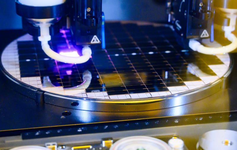
Intel has been a leader in promoting a resilient global supply chain and has been willing to pony up billions for new and improved foundry operations. The Fab 9 opening in Rio Rancho, NM., is part of Intel’s previously announced $3.5 billion investment for New Mexico advanced packaging technology. Fab 9 and Fab 11x in Rio Rancho are the first operations site for mass production of 3D advanced packaging technologies. Foveros and EMIB (embedded multi-die interconnect bridge) packaging offer a faster and more cost-efficient way to produce chips, and Intel has set a goal of 1 trillion transistors on a chip.
Intel’s ambitions include a desire to be the world’s second largest foundry by 2030. Today, TSMC is the largest, followed by Samsung, Global Foundries and UMC.
Foveros allows compute tiles to be stacked vertically, rather than side-by-side. That way, foundry customers can mix and match compute tiles with greater power efficiency and with optimum cost. Foversos was first introduced in 2019. An Intel video shows the packaging process.
The Foveros production achievement in New Mexico caught the attention of Jack Gold, analyst at J. Gold Associates. “Packaging often gets less visibility and press than the latest process node, but it’s critical to continue the pace of Moore’s Law,” he said. “With chiplets becoming a critical component of future producgts, having a domestic source for leading edge packaging, versus it mostly being done in the Far East, is important for supply chain management. This will give Intel a critical advantage in both producing its own processors as well as for its Intel Foundry Services. Potential customers of IFS will see this as a very attractive capability as they choose a contract fab supplier.”
The separate announcement of Intel’s collaboration with UMC is intended to help them address high growth markets in mobile, communications infrastructure and networking. Intel called it a “long-term agreement.” The 12 nm node will use a FinFET transistor design and be developed and made in Fabs 12, 22 and 32 at Intel’s Ocotillo site in Arizona. Product of the 12 nm process is expected to begin in 2027.
Intel’s stock price reached a high of $73.94 on Sept. 1, 2000, and a more recent high of $64.87 was reached on March 26, 2021. The price was $49.24 on Jan. 25 prior to the 2023 fourth quarter earnings call.