
In Brief
It is assumed that higher camera resolution and higher dynamic range yield better image quality. Why then do cameras with virtually identical specifications perform so differently?
The way specifications relate make them more complex than their definitions suggest. Learn keys for CCD imager evaluation that allow you to determine true functional system performance.
Understanding Resolution
The resolution of an imaging colorimeter is defined as the number of individual horizontal (M) and vertical pixels (N) captured by the imager (typically a CCD). For typical high-accuracy imaging colorimeters, multiple images are captured through different filters that mimic the x-bar, y-bar, and z-bar tristimulus curves. These images are then processed to overlap and form one image containing X, Y, and Z tristimulus values for each MxN pixel of the image. High-accuracy imaging photometers capture a single grayscale image through the y-bar filter.
In some instances, a Bayer-filter RGB camera is calibrated to measure color. These systems lack the color accuracy of a CIE filter-based system and are therefore limited to specific applications such as color uniformity. They do, however, gain a speed and cost advantage (since only one image is captured) and do not require expensive x-bar, y-bar, and z-bar filters. In this case, the effective resolution of the pixels is significantly less than a CIE filter-based system, because every other pixel is used to measure a different color, and the pixels in between colors are interpolated.
These RGB systems therefore have effectively half the resolution in the horizontal and vertical dimensions. Using an example of a 16MP CCD, the effective resolution of an RGB system is 4MP, as no new information is introduced by the interpolation. Following the same logic, a 16MP CIE filter system could claim a resolution of 64MP resolution by interpolating every other pixel. Of course, this doesn’t make any sense – but it clearly demonstrates that the resolution of these two camera types is not directly comparable.
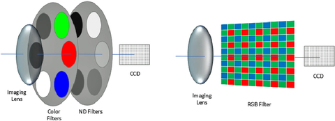
The question of resolution becomes more interesting when comparing two high-resolution CIE filter-based imaging systems. For example, given the same resolution camera, what contributes to the performance differences between different imaging systems? Are some systems better suited than others to certain applications?
To answer these questions, we need to look at signal-to-noise on a per pixel basis. Below, we’ll discuss different sources of noise in a CCD-based measurement and how these sources impact different measurement applications.
Dynamic Range Defined
There are a few units of measurement used to describe a camera’s dynamic range, which can naturally cause some confusion. For CCD-based measurements, dynamic range is commonly measured in decibels (dB) to describe the ratio of maximum possible signal-to-read noise (signal-to-noise ratio, or SNR). For the purposes of this paper, we will use this definition to describe dynamic range. Other expressions for dynamic range include bit depth of digitization (e.g., 12-bit or 14-bit) or a ratio (e.g., 10000:1).
The mathematical expression used for the dynamic range of a CCD is:

Well size is the number of electrons available in a pixel (i.e., the number of electrons available prior to CCD saturation). In this case, read noise is the electronic noise, expressed in electrons, introduced into the signal when transferring the data from the CCD into digital format. This amount is independent of light level (or saturation) of the measurement. Therefore, it is measured in the dark state (a dark frame) to separate this noise from statistical photon noise.
Let’s take an example of a CCD with a well size of 20ke- (20 kiloelectrons) per pixel and a system read noise of 12e-. Using these values, we obtain a value of 64.4 dB.
Note that we are using the expression system read noise, which differs from CCD read noise. Any electrical system taking analog data from the CCD and converting it to digital format will introduce noise. The amount of noise introduced will be dependent on the speed the data is pulled from the CCD, as well as the quality of the electrical circuit, camera design, and board manufacture.
When basing a claim of dynamic range using the above equation (1), one must consider more than the CCD manufacturer’s well size and read noise claim. The read noise must be measured from the entire camera system. Equation (1), then, is calculated based on post analog-to-digital conversion (ADC) gray count, with the read noise and well size being noise measured in gray counts and saturation level in gray counts, respectively.
Adding Shot Noise to the Equation: The Photon Transfer Curve
The equation above doesn’t tell the full story with regards to dynamic range. This is because any measurement of light is subject to an irreducible statistical measurement error, called shot noise. The ratio of this noise – and other sources of noise – can be measured in a light frame image (an image of a scene with standard saturation; for example, 50-70% of full well) using the Photon Transfer Curve (PTC) measurement technique. The PTC is a log-log plot of variance versus signal level, and is used by leading camera manufacturers and users to enable a direct comparison of key performance parameters for CCD-based imaging systems.1
Shot noise is noise based on the variation in the amount of discrete independent photons detected in a given time. This variability follows a Poisson distribution, such that for large numbers, the variability follows Gaussian statistics, or the square root of the average number of photons (electrons) measured.
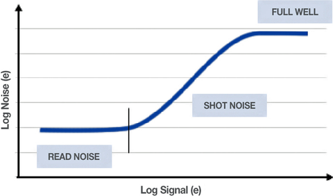
In this manner, for an image taken near full saturation, the shot noise can be expressed as √N,  with N being the well size.
In any measurement, the total noise is a combination of the independent error-contributors: shot noise, read noise, and pattern noise. Pattern noise, if repeatable, can be referred to as “Fixed Pattern Noise” (FPN). This typically can be calibrated out via flat-field or other calibration techniques. For the purposes of this paper, we will assume that pattern noise has been calibrated to the point of insignificance. However, this is not an assumption that can be casually made, as such pattern noise can be quite difficult to remove when it is not repeatable. We have observed this characteristic in certain imaging technologies, and it is one of the reasons that Radiant has not yet added CMOS sensors to its line of imaging colorimeters.
For a near-full saturation measurement, the total noise can then be expressed as:

For our example of a CCD with a well size of size of 20ke- and a read noise of 12e-, the total noise in electrons is:

As shown here, the system read noise becomes negligible as the CCD well size becomes larger.
The noise level can be expressed as a fraction of signal:

Or, conversely, the SNR can then be written as:

Using the same example, we obtain a value of 141:1 for one standard deviation for the light frame SNR of one pixel. Expressed as an error level, we obtain a value of 0.7% for one standard deviation.
Right away, we can see that if we have a light frame SNR of 141:1, we must be cautious about the bit depth claims we make on the signal. For example, claiming 16-bit dynamic range (65535:1), simply because the AD conversion yields a 16-bit signal is meaningless. In this case, the lower 8 bits on a per-pixel basis are effectively noise.
Effective Number of Bits (ENOB) is sometimes used to describe dynamic range in terms of bit depth; it is important to understand if ENOB is the value being used, or if it is simply the ADC signal.
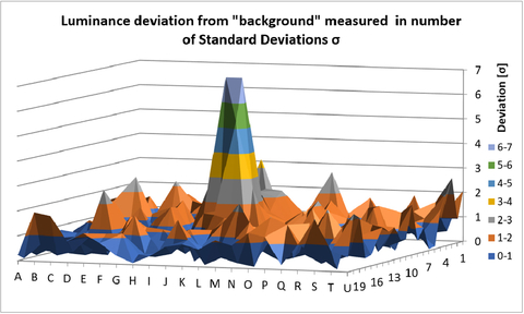
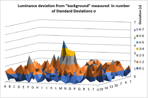
Signal-to-noise ratio (SNR) is critical when looking at subtle differences in light frame measurements. Radiant Vision Systems mura and defect detection systems, for example, rely heavily on it. Suppose we would like to detect a very small particle defect in a display that varies in contrast only slightly from neighboring areas. For the sake of the example, we’ll suppose the size of this defect is only 1x1 CCD pixel for a 29MP measurement. To repeatedly detect this defect without many false positives, the defect contrast should be 6 standard deviations beyond the CCD measurement noise level. If we use the value above for light frame noise level, 6 standard deviations of noise is 4.2%. So, for a very small particle defect, the system would increasingly confuse noise with the defect of interest as the contrast of this defect falls below 4.2%. This is illustrated in the following graphics:
How To Increase SNR
As can be seen from equation (5), the way to increase SNR is to increase the well size of the CCD pixels, while controlling noise sources. Controlling noise is done by investing in a quality imaging system. Such a system will offer a high-quality, low-noise CCD, system design that includes high-quality electronic components, and active CCD cooling. Increasing well size of the CCD pixels can be accomplished in several different ways:
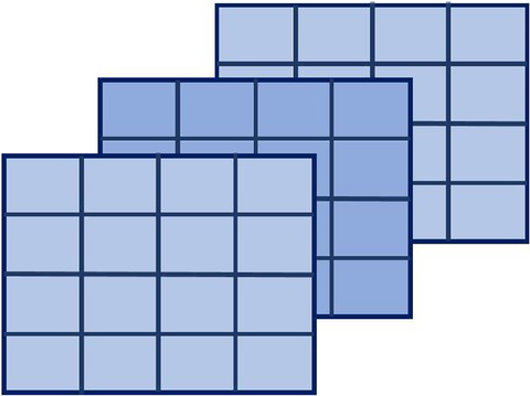
- Averaging several measurements: By repeatedly taking the same measurement over and over, it is possible to “fill up” the electron well several times, thereby effectively obtaining a larger electron well. There are two major disadvantages to this approach, however. First, averaging more measurements in repetition means longer measurement times. In a production testing setting where takt times must be met, measurement averaging is not desired. The second disadvantage to taking several measurements is that this method cannot be used for devices that are moving during measurement. When a device is imaged using a flash or very short exposure time, there is not enough time to average over multiple measurements.
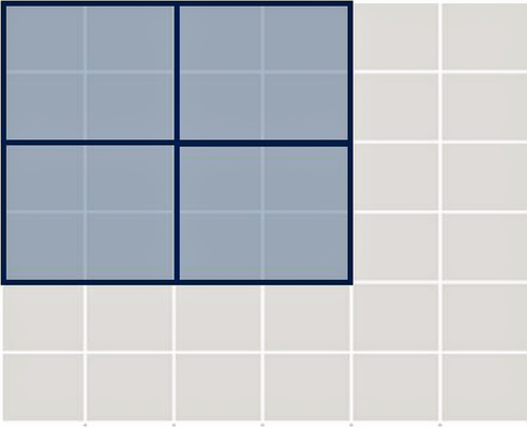
- Binning: By averaging signals over neighboring CCD pixels, it is possible to increase well size. For example, binning 2x2 means that 4 CCD pixels are combined to create effectively one pixel. In the example we have been using with a CCD well size of 20ke-, binning would yield an 80ke- pixel well size, which would provide a 2X increase in the SNR ratio to 282:1, and reduce the light frame error level to 0.35%.
However, using this method also reduces the resolution of the imaging system. We can clearly see that the resolution and signal-to-noise ratio are closely intertwined.
- Selecting CCDs with larger pixel areas: Very simply, larger pixel size means larger well size, and higher SNR. It is the great advantage of larger CCDs. However, imaging to larger CCDs can be more complex, often requiring expensive custom lenses. A standard 35mm lens, for example, will typically not supply light to the edges of a large-format CCD. On the other hand, increasing resolution by using smaller pixels is not desirable as it will decrease the SNR. When trying to maintain a high SNR without sacrificing cycle time and resolution, using larger pixels is the optimum solution.

The points above help to answer to our original question: “Given the same resolution, what parameters account for performance differences among imaging systems?” The answer is: Signal-to-noise ratio (as calculated via the photon transfer curve), on a single pixel basis, in a single measurement. This is the key performance metric, and key cost driver, for CCD-based measurement systems, when resolution is held constant.
This brings us to the second question we asked above: “Given the same resolution, are some imaging systems better suited to specific applications?” The answer is certainly yes, with the primary determining factor being the noise level required to discern the contrast level of interest.
Conclusion
We can clearly see that resolution and dynamic range play a critical role in imaging system performance. However, these specifications when considered on their own provide limited information. Additional factors, including shot noise, CCD well size, and pixel size, must be considered.
The optimal solution for high-precision measurements will be a compromise: We want enough pixels to capture an image in fine detail (resolution), but we also want to measure those fine details with high accuracy and high repeatability. A large CCD well size, with large pixel size, is critical to obtaining high-quality images in the least amount of time.
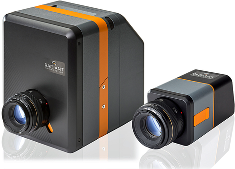
Radiant has found this to be optimal for high-precision measurements.
1Further explanations of the Photon Transfer Curve are available on the internet. Please see below for useful resources:
Additional References:
J. Janesick, “CCD transfer method - standard for absolute performance of CCDs and digital CCD camera systems”, Proceeding of SPIE, Vol.3019, 70-120, 1997.
J. Janesick, K. Klaasen and T. Elliott, “Charge-coupled-device charge-collection efficiency and the photon-transfer technique”, Optical Engineering, Vol. 26, no. 10, 972-980, 1987.
About the author
Doug Kreysar heads Radiant’s engineering, product development, and operations teams to ensure the successful implementation of customer solutions worldwide. Under his direction, Radiant’s optical technologies for light and color measurement have become known as the gold standard for production test applications. Kreysar received a BS in Physics from Vanderbilt University, and an M.S. in Applied Physics from the University of Michigan, Ann Arbor. He is author of multiple technical papers and a regular speaker in industry symposia. Kreysar has been awarded eight US patents.
Contact Info:
Radiant Vision Systems, LLC
+1 (425) 284-0152