
Over the past decade, microelectromechanical systems (MEMS) have experienced significant growth and market acceptance, driven largely by their reliability, manufacturability, and potential for low unit cost. In the coming decade, microsystems are expected to continue as a leading driver of innovation, with manufacturers and OEMs looking to incorporate small, relatively inexpensive sensors/actuators into their products to improve their performance, reliability, and longevity and to lower their cost.
 |
For the most part, silicon has been the material of choice for MEMS components. However, for an increasing number of demanding applications, silicon isn't the best construction material from a performance standpoint. For example, developing advanced engine systems requires sensors that can operate in the harsh environments near the ignition source (hot) and in the exhaust stream (hot and corrosive). This has led microsensor manufacturers to investigate advanced materials capable of operating reliably in such demanding environments. The challenge lies in bringing these microsystems based on advanced materials to market at a reasonable cost, i.e., using conventional microfabrication techniques to enable suppliers to deliver large volumes cheaply.
This article provides an overview of the advantages of silicon carbide (SiC) for such demanding microsystem applications and describes recent progress in overcoming the difficulties associated with microfabrication of SiC MEMS components.
Why Silicon Carbide?
Silicon carbide is uniquely suited to use in harsh environment sensors. Figure 1 lists the important physical properties of the leading semiconductors under investigation: silicon (Si), gallium arsenide (GaAs), SiC, and diamond. While silicon (specifically, silicon on insulator, or SOI) and GaAs can be pushed to reasonably high operating temperatures (~300°C) and radiation fluxes (1 Mrad), these two materials are not well suited for harsh mechanical and chemical environments. Neither is sufficiently rugged to form the basis for a harsh-environment MEMS platform technology. SiC and diamond stand out from other MEMS materials based on their ability to survive in harsh conditions; in contrast to other durable materials proposed for harsh environment sensors—including alumina, tantalum oxide (Ta2O5), and titanium carbide (TiC)—SiC and diamond are semiconductors and can provide both mechanical and electronic functionality. Both are wide bandgap materials, making them suitable for high-temperature operation and radiation-hard electronics. Both are extremely chemically inert (although diamond is susceptible to oxidizing environments) and mechanically hard. From a mechanical standpoint, SiC has outstanding material properties, including high elastic modulus, fracture toughness, operational stability, wear resistance, chemical inertness, and thermal conductivity. As an electronic material, SiC has a wide bandgap, high breakdown strength, and high saturation drift velocity. Significantly, the commercial viability of SiC electronic circuits is advancing rapidly as wafer size and quality increase, laying the groundwork for successful integration with SiC transducer elements. SiC's wide bandgap, coupled with its high thermal conductivity, provides for high-temperature/-power operation and radiation hardness. Based on these factors and with recent advances in SiC microfabrication technology [1], SiC is now a realistic and commercially viable platform for harsh-environment MEMS products.
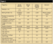 Figure 1. Looking at the various material properties, SiC and diamond are superior to silicon and GaAs if you consider the combination of thermal, mechanical, and electrical properties. In addition, SiCs mechanical and electrical properties maintain their advantage over silicon at high temperatures. |
SiC Microfabrication Progress
Commercially available SiC electronic component products, such as power transistors and Schottky diodes, continue to proliferate due to the combination of constantly improving defect densities and the availability of large-diameter SiC wafers. Reducing basal plane dislocations in substrates minimizes the growth of stacking faults in epitaxial layers, which is the key to fabricating reliable SiC bipolar devices. Advances in the quality of thick epitaxial layers make it possible to fabricate high-voltage SiC PIN diodes with better forward voltage drift, low reverse leakage, and high carrier lifetime. Similarly, MOS SiC devices offer a lower threshold voltage and higher channel mobility (approaching 100 cm2/Vs) through improved oxidation techniques and post-oxidation anneals [2]; accelerated lifetime tests predict >100 yr. of reliable operation at 300°C. 4H-SiC vertical JFETs for high-temperature applications are coming to market shortly [3]. In parallel with these developments, low-resistance ohmic contact metallization technology has been developed, and this has demonstrated stability of contact resistance for 1000 hr. in a 600°C environment [4]. In contrast, standard metallization operating in high temperatures experiences unstable contact resistance and degrades over time. Such advances in material and device quality demonstrate the commercial readiness of SiC electronic devices for use in high-temperature, high-power, or high-radiation environments where silicon devices cannot perform. Furthermore, such advances lead to an enhanced ability to fabricate SiC MEMS products with close-coupled signal-conditioning electronics that can survive in harsh environments.
In a similar fashion, significant progress has been made in developing cost-effective SiC micromachining techniques. Whereas electronic components require the use of monocrystalline SiC for its predictable electronic properties, MEMS and microstructures can be fabricated from polycrystalline SiC (poly-SiC). High-quality stoichiometric poly-SiC thin films are deposited by conventional low-pressure chemical vapor deposition (LPCVD) in multiwafer furnace systems onto a variety of substrate materials at temperatures below 1000°C. This obviates the need to start with monocrystalline SiC substrates, reducing component cost, and enables deposition of structural layers on top of common sacrificial materials such as silicon dioxide and silicon nitride. This process is inherently scalable to large batch sizes and large wafer diameters, opening up the possibility of fabricating SiC-based MEMS products for high-volume applications. Poly-SiC deposition is a versatile process that allows for excellent control and adjustability of both electrical and mechanical properties. For example, film conductivity can be controlled using in situ doping to produce highly conductive layers (e.g., <10 mW-cm). Perhaps most important for MEMS applications, the residual stress of the poly-SiC layers can be adjusted in a repeatable manner over a wide range (e.g., over stress values from 300 MPa to –100 MPa), allowing tailoring of film stress to meet particular device requirements. In addition, stress gradients as low as 1.5 x 10⁻⁵ μm–1 have been demonstrated [5]. Figure 2 shows a SEM micrograph of a released 4 μm–thick poly-SiC microstructure, in which the planarity of the suspension beams illustrates the very low stress gradient.
 Figure 2. This SEM micrograph shows released poly-SiC microstructures fabricated from a 4 μm–thick film that was photolithographically patterned and etched. The extreme flatness of the suspension beams indicates a very low stress gradient. |
Photolithography-based patterning techniques have been developed to pattern the poly-SiC films in conventional reactive ion etching (RIE) equipment with standard etch chemistries (e.g., SF6/O2); photoresist, silicon dioxide, or metal mask layers can be used [6]. SiC etch rates and etch selectivities can be comparable to those of polysilicon, although it is generally more difficult to achieve a process with high selectivity to nonmetal masking films based on the chemical "strength" of SiC. Common wet chemistries for silicon will not etch poly-SiC at a significant rate. Another approach to patterning SiC microstructures involves the use of micromolding, whereby an inverse pattern is etched into a sacrificial layer such as silicon dioxide. Poly-SiC is deposited conformally into the mold and then planarized using chemical-mechanical polishing. This approach lends itself to making multilayer SiC MEMS devices, and has been used in the multiuser silicon carbide (MUSiC) process [7] to fabricate inertial and pressure sensors, RF switches, micromirrors, and other devices. In addition to the planarization process, a fine polishing process has been developed for optical MEMS applications. It produces ultra-smooth SiC surfaces with an extremely low average roughness (RA) of 1 nm. Figure 3 is an optical micrograph of a 35 mm x 35 mm x 2 μm poly-SiC membrane fabricated on a 4 in. dia. silicon wafer. The diaphragm is extremely flat, smooth, and uniform because of the ability to control residual stress, surface roughness, and thickness uniformity.
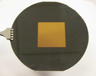 Figure 3. This image shows a 35 mm square poly-SiC membrane fabricated from a 2 μm– thick film on a 4 in. silicon wafer. The ability to control residual stress and thickness uniformity, combined with ultra-smooth polishing, results in a large-area membrane that is very flat, uniform, and transparent. This has been developed as a mask blank for next-generation lithography. |
Demanding MEMS Applications
A variety of potential harsh environment applications for SiC-based microsystems are envisioned, particularly in the power generation arena. Engine makers are developing advanced techniques to monitor and control the combustion process to further improve engine performance (i.e., fuel efficiency and lower emissions). Advanced engines are expected to need mass air flow and pressure sensors placed in the exhaust stream to provide real-time, accurate feedback on engine performance.
SiC microbridge heater arrays have been fabricated as the basis for hot-wire anemometer flow sensors. These heaters require very low power (becoming incandescent under applied voltages as low as 15 V), and have fast response due to SiC's high thermal conductivity. It is easy to envision a surface micromachined multisensor chip that contains both of these elements integrated monolithically.
Based on advances in commercialization of both SiC electronic components and SiC-based MEMS transducer elements, new microsystem products for demanding applications are closer to becoming a reality. Development of cost-effective batch processing techniques combined with SiC's superior material properties provide a compelling argument for silicon carbide as the new material of choice for microsystems.
MUSiC is a registered trademark of FLX Micro.
References
1. M. Mehregany, C.A. Zorman, N. Rajan, and C. H. Wu, "Silicon Carbide MEMS for Harsh Environments," Proc IEEE, Vol. 86, pp. 1594-1610, 1998.
2. M.K. Das, "Recent Advances in (0001) 4H-SiC MOS Device Technology," Proc 10th International Conference on Silicon and Related Materials 2003, Lyon, France, Oct. 5-10, 2003.
3. I. Sankin, J.N. Merrett, W.A. Draper, J.R.B. Casady, and J.B. Casady, "A review of SiC power switch: achievements, difficulties and perspectives," Proc 10th International Conference on Silicon and Related Materials 2003, Lyon, France, Oct. 5-10, 2003.
4. R.S. Okojie, D. Lucko, and D. Spry, "Reliability of Ti/TaSi /Pt ohmic contacts on 4H- and 6H-SiC after 1000 hours in air at 600 C," Proc Electronic Materials Conference, Notre Dame, IN, June, 2001, p. 6.
5. J.M. Melzak, C.H. Wu, E.M. Zdankiewicz, "Silicon Carbide for Demanding MEMS Applications," Proc Sensors Expo Conference, Detroit, MI, June 9, 2004.
6. D. Gao, M.B.J. Wijesundara, C. Carraro, R.T. Howe, and R. Maboudian, "Percent Progress Toward a Manufacturable Polycrystalline SiC Surface Micromachining Technology," IEEE Sens. J., Vol. 4, No. 4, pp. 441-448, 2004.
7. J.M. Melzak, A. Leppart, S. Rajgopal, and K.M. Moses, "MUSiC—An Enabling Microfabrication Process for MEMS," Commercialization of Micro Systems Conference (COMS 2002), Ypsilanti, MI, September 8-12, 2002. ?
Jeffrey M. Melzak is Vice President of Engineering and Chien-Hung Wu is Director of Process Engineering, FLX Micro, Solon, OH; 440-498-4300, [email protected], [email protected], www.flxmicro.com.