Capacitive Micromachined Ultrasonic Transducers (CMUT) are MEMS (Micro-Electro-Mechanical-Systems) based structures that can be used to generate and sense acoustic signals in the ultrasonic range. Ultra high-resolution, wide-bandwidth and highly miniaturized ultrasound transmitters and receivers can be realized with CMUTs. These devices can be mass produced using silicon micromachining techniques and lend themselves to chip-scale integrations with driver ASICs. In addition to miniaturization and superior imaging resolution CMUTs are highly reliable devices even at high temperatures; conditions where typically conventional ultrasound transducers tend to fail.
CMUTs, first invented in the mid 1990’s [1], are gaining adoption in ultrasound systems. CMUT based systems have recently been announced as a one-probe solution for a wide range of ultrasound examinations in both high-end ultrasound systems (Hitachi, [2]); as well as enabling a new generation of pocket-sized, whole body imaging ultrasound systems such as the Butterfly iQ [3].
Advantages of CMUTs versus conventional Lead Zirconium Titanate (PZT) in medical imaging systems
CMUTs offer many potential advantages over conventional PZT transducer materials, which dominate present ultrasound products.
- CMUTs offer better acoustic matching to the propagation medium, resulting in wider immersion bandwidth and improved image resolution
a. Frequency range from 500 kHz to 50 MHz tunable by precision dimensional control
b. Multiple frequency elements can be placed in a single array with one process
- CMUTs are lead free, ROHS compliant, with no toxic materials, which is especially advantageous for invasive ultrasound, unlike lead based PZT devices
- Ability to be integrated with electronic circuits in chip-scale packages thus enabling miniaturization, leading to smaller form factors and more reliable and robust designs
- A natural solution for 3D imaging through the realization of 2D CMUT arrays
- Ease of manufacturing and expected reduction in production costs – silicon micromachining techniques replace labor-intensive, element based assemblies of conventional PZT handheld linear arrays
- Higher sensitivity and wide bandwidth operation of CMUTs make them an ideal solution for photoacoustic imaging
![Sensors Insights 2018-06-19 Fig1 Fig. 1: Ultrasound transducer from Butterfly Network Inc. [4] Whole body imaging with a single transducer. Retails under $2k.](https://qtxasset.com/styles/breakpoint_sm_default_480px_w/s3fs/sensorsmag/1529179916/FIG_1.jpg/FIG_1.jpg?itok=b-BrpMSI)
CMUT - Imaging Applications
Today's ultrasound technology covers a wide range of measurements, diagnostic, and other applications, e.g. from non-destructive testing to medical ultrasound imaging or from surveillance in process plants to distance measurement. Each of these areas can be implemented more efficiently using CMUTs versus conventional PZTs.
In addition, CMUTs are receiving increasing acceptance as an alternative to piezoelectric transducers for new fields of applications due to many distinctive features. While not an exhaustive list, some of them are listed below:
- Photoacoustic imaging - Photoacoustic imaging is a hybrid modality, combining the high-contrast and spectroscopic-based specificity of optical imaging with the high spatial resolution of ultrasound imaging
- Medical therapy - High intensity focused ultrasound (HIFU) is a treatment that aims to kill cancer cells with high frequency sound waves.
- Guidance for therapeutic ultrasound
- Affinity sensor for immunosensing
- Ultrasound microscopy
CMUT - Principle of operation
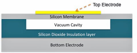
The CMUT is a MEMS structure comprising of two electrodes facing each other; one of which is fixed and the other is movable. An insulating layer and a vacuum-sealed gap separates the two electrodes.

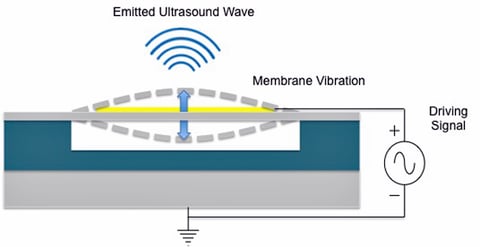
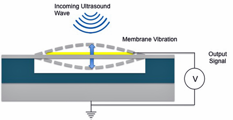
CMUTs can operate in transmit and receive mode, by converting electrical energy into acoustic energy or vice versa through the displacement of the movable electrode.

In the transmit mode, an alternating voltage is applied between the membrane and the substrate back plate. The resulting electrostatic forces deflect the movable electrode towards the fixed one, thus generating an acoustic wave at the frequency of modulation.

In receive mode, an ultrasonic wave causes membrane vibration and a change of capacitance, which can be detected. This change in capacitance can be sensed and digitally processed to generate an image for further analysis.
This relative change in capacitance is characterized by a term called k squared effective, where the static capacitance is CT and the moving capacitance is CS, given in this equation: keff2 = ( CT - CS )/ CT = 1 - CS/CT
This coupling coefficient (or factor) k is effectively the untuned transduction efficiency. A perfect device would have a maximum coupling coefficient of 1. Conventional ultrasound transducers have coupling coefficients of 0.42, while the more expensive single crystal ones can be as high as 0.68. CMUTs developed at Micralyne have shown coupling coefficient of 0.75.
Additional sensitivity and efficiency can be achieved by “collapse-mode” architectures [6]. In the collapse-mode operation, the membrane is biased more than the pull-in voltage, resulting in the center part of the membrane to contact with the bottom electrode. A CMUT cell thus effectively acts as a ring-shape transducer. The electric field strength in the cavity is higher in the collapse-mode CMUT compared to the conventional CMUT, thus collapse-mode operation provides better transmit and receive efficiency.
Other architectures to enhance transducer efficiency include the Multiple Moving Membrane Capacitive Micromachined Ultrasonic Transducer (M3-CMUT). This design consists of two deflectable membranes and one static electrode [7].
CMUT Fabrication at Micralyne
Micralyne offers advanced prototyping, development and volume manufacturing services for CMUTs, both for components and for complete module assemblies.
Micralyne’s patented CMUT design [8] uses a doped Silicon-on-Insulator (SOI) and wafer bonding fabrication method described in Figure 5, and is composed of semiconductor layers, insulator layers, and metal layers. Conventional doped silicon may be used as the electrode layers. Other suitable semi-conductor materials such as silicon carbide may alternately be used for the electrode layers. The insulator can be made of silicon oxide, silicon nitride, or other suitable dielectrics.
Micralyne’s CMUT technology enables high volume ultrasound transducer manufacturing at a lower cost compared to current solutions. Customers benefit from the extensively tested pre-characterization and validated process flows in place at Micralyne, allowing fast-track design projects, savings months of development time. Value-add assembly solutions from Micralyne such as Wafer Level Packaging (WLP) and Through Silicon Vias (TSV) further enable customers to design highly efficient, extremely miniaturized medical imaging systems.
![Sensors Insights 2018-06-19 Fig5 Fig. 5: Process flow for CMUT fabrication at Micralyne [5]; (a) The top Boron-doped Si layer of an SOI wafer is patterned to form electrodes with an insulating SiO2 base; (b) thermal oxide growth; (c) patterning of oxide layer to define CMUT cavities and](https://qtxasset.com/styles/breakpoint_sm_default_480px_w/s3fs/sensorsmag/1529180302/FIG_5.jpg/FIG_5.jpg?itok=-z7uLf4A)
CMUT Integration with ultrasound imaging ASICs
Close integration of ultrasonic transducer arrays and supporting integrated circuits is highly desired in many applications, especially for transducer arrays with small elements such as in 2D arrays and arrays for use at the end of a catheter.

Ultrasound transducers are the key signal generating and receiving component in ultrasound imaging systems. In conventional ultrasound systems, these transducers are fabricated from thin layers of PZT and composite acoustic materials, bonded together and diced into elements. These are complex and precise labor-intensive systems with yield and reliability challenges. Costs of these assemblies go up dramatically when designing 2D arrays. The traditional transducer architecture is thus difficult to build, lacks robustness and remains cost-challenged for larger 2D arrays.
CMUTs offer an attractive alternative to break free of the labor-intensive, element based architectures of today. Advantages in underlying fabrication techniques make CMUTs a superior option for use in next-generation imaging systems. CMUT technology uses integrated circuit (IC) processing techniques to fabricate arrays of ultrasonic transducers in different forms and sizes. Basic silicon micromachining and batch processing techniques allow thousands of arrays to be fabricated at once with each production run. Arrays with different operating frequencies, different numbers of elements, and even different geometries can be fabricated on a single silicon wafer, resulting in both uniform quality and reduced cost. Batch manufacturing provides significant cost reduction compared to existing PZT transducer fabrication technology. CMUT technology also conveniently integrates the transducer array with supporting ultrasound imaging circuits by directly bonding to the ASICs using well established flip-chip bonding processes, thus offering high-quality and highly reliable systems.
References:
- M. I. Haller and B. T. Khuri-Yakub, “A surface micromachined electrostatic ultrasonic air transducer,” in Proc. IEEE Ultrason. Symp., Feb. 1994, pp. 1241–44.
- Hitachi to launch “ALOKA ARIETTA 850”, the flagship model of the ARIETTA series diagnostic ultrasound platforms, http://www.hitachi.com/New/cnews/month/2017/03/170302a.html
- New "Ultrasound on a Chip" Tool Could Revolutionize Medical Imaging, IEEE Spectrum, 27 Oct 2017, https://spectrum.ieee.org/the-human-os/biomedical/imaging/new-ultrasound-on-a-chip-tool-could-revolutionize-medical-imaging
- Butterfly Network Inc., Butterfly iQ Ultrasound on a chip, https://www.butterflynetwork.com/
- P. Zhang, G. Fitzpatrick, T. Harrison, W. A. Moussa and R. J. Zemp, "Double-SOI Wafer-Bonded CMUTs With Improved Electrical Safety and Minimal Roughness of Dielectric and Electrode Surfaces," in Journal of Microelectromechanical Systems, vol. 21, no. 3, pp. 668-680, June 2012. doi: 10.1109/JMEMS.2012.2189358
- Oralkan, O & Bayram, Baris & Yaralioglu, G.G. & Ergun, Sanli & Kupnik, Mario & Yeh, David & O. Wygant, Ira & Khuri-Yakub, Pierre. (2006). Experimental Characterization of Collapse-Mode CMUT Operation. Ultrasonics, Ferroelectrics and Frequency Control, IEEE Transactions on. 53. 1513-1523. 10.1109/TUFFC.2006.1665109.
- Arezoo Emadi, Tahereh & Buchanan, Douglas. (2013). Design and fabrication of a novel MEMS capacitive transducer with Multiple Moving Membrane, M3-CMUT. Submitted to IEEE Transactions on Electron Devices. 61. 10.1109/TED.2013.2297677.
- US Patent US20120086087A1, Fitzpatrick Glen A., SOI-based CMUT device with buried electrodes, https://patents.google.com/patent/US20120086087
About the author
Glen Fitzpatrick has worked at Micralyne for more than 30 years, and currently serves as the Chief Scientific Officer for the company. Glen joined Alberta Microelectronic Centre (AMC) in 1987, which subsequently became Micralyne in 1998. Glen focuses on MEMS innovations and bringing best practices to the solutions offered to Micralyne’s customers. His role is to advance Micralyne’s state-of-the-art and emerging trends in MEMS technology at the device, process, and equipment levels. He is also a principal internal consultant on device design and performance, and fabrication process development and troubleshooting.
Glen has spearheaded several breakthrough MEMS technologies, including developed processes for glass micromachining for microfluidics, and has contributed to a textbook on the topic. He also has designed and has patents awarded for high speed (10 MHz), electrically configurable linear array diffraction gratings, as well as for all-silicon ultrasonic transducer (CMUT) devices. His prior work includes designing a glass/silicon-based architecture for micro-mirror devices, which were used in telecom applications.
Glen has Bachelor of Science degrees in both Mechanical and Electrical Engineering.