

An about-face in the march toward increasingly expensive geometry miniaturization signals a new era of development and manufacturing for microelectronics. The recent trend toward large-scale integration of materials focuses a broad range of commercial and government interests on the More-than-Moore (MTM) approach for exploiting the massive number of available combinations of elements and novel technologies with which to accelerate systems integration.
If you've not yet heard that there may be as many as a trillion sensors utilized to drive the Internet of Things (IoT) by 2025, here's some added good news: we now have the means to make it happen sooner than that.
For the past 50 years, the microelectronics industry has collectively built an infrastructure that is designed to enable ever-smarter semiconductors with near-atomic-level features. However, the increasingly exorbitant price of pursuing the traditional Moore's Law approach is radically reducing the ability of the majority of companies in our world to afford that route.
In a shift toward a sensor-connected planet, a transformation in materials is underway that facilitates myriad new compounds and their applications. This revolution is about to fuel an unprecedented range of capabilities that allow game-changing applications such as more highly advanced energy-harvesting technology, infrared sensors, phased-array radars, unmanned transportation systems, and benefits for nearly every area of high relevance to society's future.
Recall that Moore's Law, named after Intel Corporation co-founder Gordon Moore, forecasts that the number of transistors that can be placed on an IC doubles every two years. In a notable departure from that historic focus, the IoT seeks to be centered on new sensor materials and how to network them.
Heralding a device-level tsunami, analysts predict that by 2020 as many as 75 billion connected devices will depend on state-of-art MEMS and other key factors like the 2.5 and 3D technologies that will enable integration for advanced sensors and novel materials.
The rapidly emerging class of materials and technologies — known as More-Than-Moore (MTM) — is being used to strategically integrate components that can yield a greater productivity than when they are positioned individually apart. To exploit this new pool of technology, nanoelectronics communities are presented with an exponentially greater number of resources that offer a significant advantage over traditional silicon foundry technologies. As a result, MTM is fast becoming the de facto solution for commercial and defensive applications. By extension, component integration will accelerate the systems integration envisioned by IoT (see figs. 1 and 2).
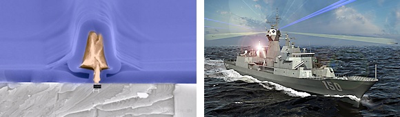
Figs. 1 & 2: Leveraging heterogeneous integration of materials like Gallium Nitride (GaN) on Silicon, improved versions of infrared imaging sensors can combine with Phased Array Radar to affordably enable greater accuracy for detecting and identifying ground and air movements for commercial and security applications.
Why The Change?
With fewer and fewer organizations able to afford to play the extremely expensive game of constantly shrinking process geometries dictated by Moore's Law, most device manufacturers are opting not to recapitalize to pursue deep submicron nodes. Thus, much of the older technology and tools found in many of the existing fabs limit their ability to develop future generations of high-demand technologies such as lab-on-a-chip devices, microbolometers, and advanced types of chemical sensors.
In response to this reduced capacity, a notable part of the trend toward utilizing MTM is for a wide range of industries to use third-party resources that cleverly leverage current technologies into next-generation solutions. Previously dismissed as being too exotic, thousands of new combinations of elements are being used to produce microfluidics, novel transistors and photovoltaics. Playing a pivotal role in this evolution, a handful of nanofabs have begun to produce such high-demand apps as genomic sensing and sequencing devices, the next generation of high-resolution microbolometers, and through-silicon vias (TSVs) for infrared sensing, that help to meet the vision for a robust IoT.
For instance, several companies are working on novel sensor technologies whereby doctors can prescribe "smart sensor pills" for their patients that double as ingestible sensors, wirelessly reporting back on the body's vital signs. A version of these sensors has been created to track what drugs patients have taken. This system consists of a pinhead-sized sensor embedded in a pill, and a battery-powered patch that monitors various health indicators, such as sleep, activity, respiration and heart rate.
No batteries are required since the sensor is powered by the human body. After being swallowed, the device transmits a signal to the patch, indicating the time of ingestion and type of pill swallowed. The patch periodically sends all of its data to a smartphone, providing doctors a way to accurately measure how patients respond to medications over time. Future versions of the smart pills will contain both medication and sensors and add the ability to measure core body temperature.
Other critical electronic advancements made possible by MTM include new ways of managing extremely complicated or open-ended tasks in short periods of time, as well as accelerated machine intelligence that can rapidly improve system capabilities. The potential is unlimited for the previously unimagined combinations to drive widespread changes and progress for the microelectronics industry.
The fast-growing set of novel and extended capabilities for connecting the IoT signals that MTM is the key to a future where nanofabrication facilities with multiple elements will pave the way. As an indication of the market to be seized, more than 85% of things — such as consumer, manufacturing, healthcare and transportation — are not yet connected today. This presents a leap forward in opportunities for the life sciences, security and defense, clean energy, consumer products, and semiconductor communities.
What The Art Of Future Development Looks Like
The majority of CMOS fabs have traditionally limited customers to working with no more than 25 elements from the Periodic Table. In profound contrast, the new class of nanofabs targeted for MTM applications will offer to synthesize solutions with 60 or more of the exotic materials (see Figure 3).
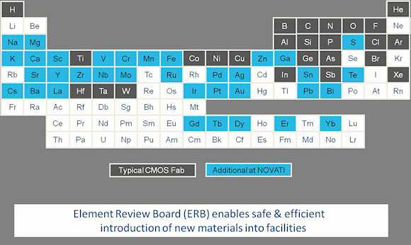
Fig. 3: Previously regarded as too exotic, thousands of new combinations of elements are being used to develop novel microelectronics that gain unique benefits from Novati's integrated materials. This new portfolio works with 60 elements from the periodic table, compared to the 25 provided by traditional foundries.
The break from the past limitations will be paved by the ability to safely engage an unprecedented number of elements in order to move innovative ideas and breakthrough designs into development and production. Novati Technologies is one example of the new type of nanofab that is among the first to offer this level of expanded product development for global applications.
Those previously under-utilized elements from the Periodic Table are being used to create new ingredients for microelectronics in areas that include silicon photonics, non-volatile memory, superconducting/quantum computing devices, GaN-on-Silicon power discretes, flexible semiconductors, and carbon nanotube electronics. To accelerate integration of next-generation sensors, Novati leverages its processing infrastructure for advanced materials, and 2.5/3D technology portfolio for customers who aim to participate in IoT. The company's utilization of TSVs and interposers allows customers to employ a much higher level of device integration to deliver better I/O speed and reduced size and power consumption from advanced sensors.
One of the approaches available to help further the development of the IoT provides for use of 3D assembly, wafer-level bonding, for example, to help heterogeneously integrate dissimilar materials and substrates to produce high-performance devices. The next generation of sensors and the products with which they'll integrate can rely on novel means to prototype new devices and then need only to run low-volume, higher-reliability upgrades for existing systems.
No Sensor Left Unconnected
Like the new markets they're helping to create, MTM-class nanofabs offer their commercial partners more ways than before to succeed at microelectronics development. One way of enabling organizations to improve the performance of their systems is through advanced packaging technology, stacking multiple chips in a single 3-D systems-in-a-package (SIP). This higher level of device integration enables miniaturization and improved power efficiency for products that contribute to the IoT.
As another example of recent sensors developed with the MTM approach at the nanofab, the incredibly sensitive "dog's nose" is the type of state-of-art app gaining broad interest for measurement and detection of chemical substances. One of Novati's customers utilized the nanofab's available materials integration to create a breathalyzer for monitoring and instantly diagnosing glucose levels in diabetics and other analyses that previously required several hours or days in a sophisticated lab.
On a much larger sized app, a further illustration of materials integration is reflected in satellite manufacturers who are driving the use of new types of non-volatile memory for storage applications on spacecraft. These latest-generation memory devices are integrating non-traditional materials and technologies to make them able to operate in high-radiation environments found in space. A few of the technologies currently being developed include Ferroelectric RAM (FeRAM), Magnetoresistive RAM (MRAM), PhaseChange RAM (PCRAM), and Resistive RAM (RRAM), all using MTM technologies.
A notable enhancement provided by the most progressive nanofabs is the allowance of customers to work side-by-side with nanofab employees inside the cleanroom to develop their new technologies, a practice that's more uncommon than one would imagine. As beneficiaries of these many improvements for device development, large corporations, small startup ventures, university spin-offs and defense contractors alike have asked for creation of such a strategic nanofabrication model. The result is a new industry standard for exploitation of designs and advantages that more traditional venues or university labs are simply not able to offer.
The Result
In summary, the fast-growing set of novel and extended capabilities for accelerating the IoT signals that MTM is the key to a future where nanofabrication facilities with multiple elements will open the way. Consequently, the radical improvement will provide the microelectronics ecosystem with more valuable sensors and MEMS that will accelerate new markets and quality of life for businesses, governments and their customers.
The era for enabling the most rapid, but affordable, product development and deployment has begun.
About the Author
Dave Anderson is CEO of Novati Technologies, a nanofabrication center providing the world's largest portfolio of elements from the periodic table to more than 100 customer organizations and companies. An ITAR-registered nanofab based in Austin, Texas, the company provides prototyping for commercial, clean energy, security and defense communities.