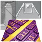
Asylum Research unveils Scanning Microwave Impedance Microscopy (sMIM), which it describes as an atomic force microscopy (AFM) technique that enables nanoscale mapping of permittivity and conductivity with unprecedented sensitivity and resolution on any material. These materials include conductors, semiconductors, and insulators. Nanoelectrical AFM modes have long been used in microelectronics R&D applications because they can provide valuable insight into device structure, function and failure. However, most conventional modes have been limited to measuring either resistance or capacitance and have required laborious sample preparation. In response, sMIM promises to be a dramatic improvement on these technologies because it senses sample variations in both conductivity (resistance) and permittivity (capacitance) while requiring only minimal sample preparation. These capabilities also make sMIM applicable to a broader range of samples, including ferroelectrics, piezoelectrics, and low-dimensional nanomaterials like graphene, boron nitride, and molybdenum disulphide. For more details, go to http://www.asylumresearch.com/Products/sMIM/sMIM.shtml.
Asylum Research
Santa Barbara, CA
888-472-2795
805-696-6466
[email protected]
http://www.asylumresearch.com