
If you make or use sensors, your business will likely feel the impact of current and future developments in nanotechnology, a very promising new branch of small-scale technology named for the unit of measure at which it operates: the nanometer, or 0.001 micron. Nanotechnology enables us to create functional materials, devices, and systems by controlling matter at the atomic and molecular scales, and to exploit novel properties and phenomena [1]. Consider that most chemical and biological sensors, as well as many physical sensors, depend on interactions occurring at these levels and you'll get an idea of the effect nanotechnology will have on the sensor world.
The trend toward the small began with the miniaturization of macro techniques, which led to the now well-established field of microtechnology. Electronic, optical, and mechanical microtechnologies have all profited from the smaller, smarter, and less costly sensors that resulted from work with ICs, fiber optics, other micro-optics, and MEMS (microelectromechanical systems). As we continue to work with these minuscule building blocks, there will be a convergence of nanotechnology, biotechnology, and information technology, among others, with benefits for each discipline. Substantially smaller size, lower weight, more modest power requirements, greater sensitivity, and better specificity are just a few of the improvements we'll see in sensor design.
Nanosensors and nano-enabled sensors have applications in many industries, among them transportation, communications, building and facilities, medicine, safety, and national security, including both homeland defense and military operations. Consider nanowire sensors that detect chemicals and biologics [2], nanosensors placed in blood cells to detect early radiation damage in astronauts [3], and nanoshells that detect and destroy tumors [4]. Many start-up companies are already at work developing these devices in an effort to get in at the beginning. Funding for nanotechnology increased by more than a factor of 5 between 1997 and 2003, and is still on the rise [5]. So this is a good time to examine the possibilities—and the limitations—of this small new world.
Possibilities
The current global enthusiasm for nanotechnology is an offshoot of several late 20th century advances. Of particular importance was the ability to manipulate individual atoms in a controlled fashion—a sort of atomic bricklaying—by techniques such as scanning probe microscopy. Initial successes in producing significant amounts of silver and gold nanoparticles helped to draw even more attention, as
|
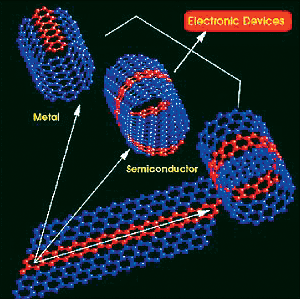
Another major contributor was the creation of carbon nanotubes (CNTs), extremely narrow, hollow cylinders made of carbon atoms. Both single- and multi-walled CNTs could, for example, be functionalized at their ends to act as biosensors for DNA or proteins. The single-walled versions can have different geometries (see Figure 1). Depending on the exact orientation of the carbon atoms, a CNT can exhibit either conducting (metallic) or semiconducting properties. This characteristic, and the ability to grow CNTs at specific locations and manipulated afterward, make it likely that the tubes will be important for electronics and sensors. For instance, they can be used in the fabrication of nano field-effect transistors for electronics or as biological probes for sensors, either singly or as an array.
Increasingly Integrated Technologies. The technologies associated with materials, devices, and systems were once relatively separate, but integration has become the ideal. First, transistors were made into ICs. Next came the integration of micro-optics and micromechanics into devices that were packaged individually and mounted on PCBs. The use of flip chips (where the chip is the package), and placement of passive components within PCBs, are blurring the distinction between devices and systems. The high levels of integration made possible by nanotechnology has made the (very smart) material essentially the device and possibly also the system. Larry Bock, chief executive for Nanosys, recently noted that "nanotech takes the complexity out of the system and puts it in the material" [6].
We can now seriously contemplate sensing the interaction of a small number of molecules, processing and transmitting the data with a small number of electrons, and storing the information in nanometer-scale structures. Fluorescence and other means of single-molecule detection are being developed. IBM and others are working on data storage systems that use proximal probes to make and read nanometer-scale indentations in polymers. These systems promise read/write densities near 1 × 1012 bits/sq. in., far in excess of current magnetic storage capabilities [7]. Although presenting a significant challenge, integration of nano-scale technologies could lead to tiny, low-power, smart sensors that could be manufactured cheaply in large numbers. Their service areas could include in situ sensing of structural materials, sensor redundancy in systems, and size- and weight-constrained structures such as satellites and space platforms.
Nanomaterials and nanostructures are other promising application areas. Two functions often separated in many sensors, especially those for chemicals and biological substances, are recognition of the molecule or other object of interest and transduction of that recognition event into a useful signal. Nanotechnology will enable us to design sensors that are much smaller, less power hungry, and more sensitive than current micro- or macrosensors. Sensing applications will thus enjoy benefits far beyond those offered by MEMS and other microsensors.
Manufacturing Advances. Recent advances in top-down manufacturing processes have spurred both micro- and nanotechnologies. Makers of leading-edge ICs use lithography, etching, and deposition to sculpt a substrate such as silicon and build structures on it. Conven.tional microelectronics has approached the nanometer scale—line widths in chips are near the 100 nm level and are continuing to shrink. MEMS devices are constructed in a similar top-down process. As these processes begin working on smaller and smaller dimensions, they can be used to make a variety of nanotechnology components, much as a large lathe can be used to make small parts in a machine shop.
In the nano arena, various bottom-up methods use individual atoms and molecules to build useful structures. Under the right conditions, the atoms, molecules, and larger units can self-assemble [8]. Alternatively, directed assembly can be used [9].
In either case, the combination of nano-scale top-down and bottom-up processes gives materials and device designers a wide variety of old and new tools. Designers can also combine micro- and nanotechnologies to develop new sensor systems.
Computational Design. Recently developed experimental tools, notably synchrotron X-radiation and nuclear magnetic resonance, have revealed the atomic structures of many complex molecules. But this knowledge is not enough; we need to understand the interactions of atoms and molecules in the recognition and sometimes the transduction stages of sensing. The availability of powerful computers and algorithms for simulating nano-scale interactions means that we can design nanosensors computationally, and not just experimentally, by using the molecular dynamics codes and calculations that are already fundamental tools in nanotechnology.
Realities
Although the excitement over nanotechnology and its prospective uses is generally well founded, the development and integration of nanosensors must take into account the realities imposed by physics, chemistry, biology, engineering, and commerce. For example, as nanotechnologies are integrated into macro-sized systems, we'll have to provide for and control the flow of matter, energy, and information between the nano and macro scales.
The Usual Design Problems—Intensified. Many of the design considerations for nanosensors are similar to those for microsensors, notably interface requirements, heat dissipation, and the need to deal with interference and noise, both electrical and mechanical. Each interface in a microsystem is subject to unwanted transmission of electrical, mechanical, thermal, and, possibly, chemical, acoustical, and optical fluxes. Dealing with unwanted molecules and signals in very small systems often requires ancillary equipment and low-temperature operation to reduce noise. Flow control is especially critical in chemical and biological sensors into which gaseous or liquid analytes are brought and from which they are expelled. Furthermore, the very sensitive, tailored surfaces of these sensors are prone to degradation from the effects of foreign substances, heat, and cold. But the ability to install hundreds of sensors in a small space allows malfunctioning devices to be ignored in favor of good ones, thus prolonging a system's useful lifetime.
|
Risk and Economics. The path from research to engineering to products to revenues to profits to sustained commercial operations, difficult for technologies of any scale, is particularly challenging for nanotechnologies. One major impediment to their adoption is the common reluctance to specify new technologies for high-value systems. Another is that at present most nano-scale materials are hard to produce in large volumes, so unit prices are high and markets are limited. Costs will decrease over time, but small companies may have a struggle making their profit goals quickly enough to survive.
|
Applications
Few sensors today are based on pure nanoscience, and the development of nano-enabled sensors is in the early stages; yet we can already foresee some of the possible devices and applications. Sensors for physical properties were the focus of some early development efforts, but nanotechnology will contribute most heavily to realizing the potential of chemical and biosensors for safety, medical, and other purposes. Vo-Dinh, Cullum, and Stokes recently provided an overview of nanosensors and biochips for the detection of biomolecules [10].
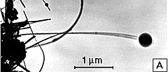
Physical Sensors. Researchers at the Georgia Institute of Technology led by Walter de Heer devised the world's smallest "balance" (see Figure 2) by taking advantage of the unique electrical and mechanical properties of carbon nanotubes [11,12]. They mounted a single particle on the end of a CNT and applied an electrical charge to it. Acting much like a strong, flexible spring, the CNT oscillated, without breaking, and the mass of the particle was calculated from changes in the resonance vibrational frequency with and without the particle. This approach may allow the mass of individual biomolecules to be measured.
|
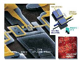
Electrometers. Cleland and Roukes at the California Institute of Technology reported the fabrication and characterization of a working, submicron mechanical electrometer [13]. This device (see Figure 3) has demonstrated charge sensitivity below a single electron charge per unit bandwidth (~0.1 electrons/ Hz at 2.61 MHz), better than that of state-of-the-art semiconductor devices.
Chemical Sensors. Various nanotube-based gas sensors have been described in the past few years. Modi et al. have developed a miniaturized gas ionization detector based on CNTs [14]. The sensor could be used for gas chromatography. Titania nanotube hydrogen sensors [15] have been incorporated in a wireless sensor network to detect hydrogen concentrations in the atmosphere. And Kong et al. have developed a chemical sensor for gaseous molecules such as NO2 and NH3 that is based on nanotube molecular wires [16].
|
Datskos and Thundat used a focused ion beam technique to fabricate nanocantilevers (see Figure 4) and have developed an electron transfer transduction approach to measure cantilever motion [17]. The results might be sensitive enough to detect single chemical and biological molecules. Structurally modified semiconducting nanobelts of ZnO have also been demonstrated applicable to nanocantilever sensors [18].
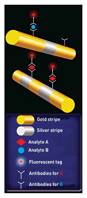
Biosensors. Nanotechnology will also enable the very selective, sensitive detection of a broad range of biomolecules. By using the sequential electrochemical reduction of the metal ions onto an alumina template, we can now create cylindrical rods made up of metal sections 50 nm to 5 microns long [19,20]. These particles, trademarked Nanobarcodes (see Figure 5), can be coated with analyte-specific entities such as antibodies for selective detection of complex molecules. DNA detection with these nano-scale coded particles has also been demonstrated.
Researchers at NASA Ames Research Center have taken a different route [21]. They cover the surface of a chip with millions of vertically mounted CNTs 30–50 nm in dia. (see Figure 6). When the DNA molecules attached to the ends of the nanotubes are placed in a liquid containing DNA molecules of interest, the DNA on the chip attaches to the target and increases its electrical conductivity. This technique, expected to reach the sensitivity of fluorescence-based detection systems, may find application in the development of a portable sensor.
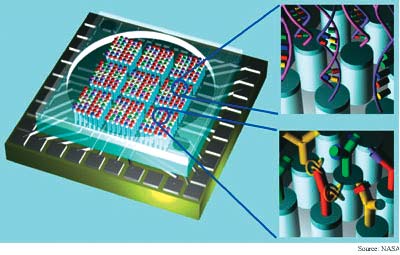 Figure 6. Vertical carbon nanotubes are grown on a silicon chip. DNA molecules attached at the ends of the tubes detect specific types of DNA in an analyte. (Courtesy of NASA Ames Research Ctr., Moffett Field, CA.) |
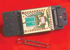
Deployable Nanosensors. The SnifferSTAR, a lightweight, portable chemical detection system (see Figure 7), is a good example of nanotechnology's potential for field applications [22]. This unique system combines a nanomaterial for sample collection and concentration with a MEMÄ-based chemical lab-on-a-chip detector. SnifferSTAR will likely find work in defense and homeland security and is ideal for deployment on unmanned systems such as micro unmanned aerial vehicles.
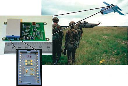 Figure 7. The SnifferSTAR is a nano-enabled chemical sensor integrated into a micro unmanned aerial vehicle. (Courtesy of Sandia National Laboratories, Albuquerque NM, and Lockheed Martin Corp.) |
And More. Other areas we expect to benefit from nanotechnology-based sensors include transportation (land, sea, air, and space); communications (wired and wireless, optical, and RF); buildings and facilities (homes, offices, factories); humans (especially for health and medical monitoring); and robotics of all types. We'll also see nano-enabled sensors increasingly integrated into commercial and military products. Many new companies will make nano materials and some will make sensors based on them. The URLs of some of these companies are given after the Reference listings.
Summary
Nanotechnology is certain to improve existing sensors and be a strong force in developing new ones. The field is progressing, but considerable work must be done before we see its full impact. Among the obvious challenges are reducing the cost of materials and devices, improving reliability, and packaging the devices into useful products. Nevertheless, we are beginning to see nano-scale materials and devices being integrated into real-world systems, and the future looks very bright indeed for technology on a tiny scale.
References
1. "Small Wonders, Endless Frontiers: A Review of the National Nanotechnology Initiative," National Academy Press, 2002.
2. Cui, Y., et al., "Nanowire Nanosensors for Highly Sensitive and Selective Detection of Biological and Chemical Species," Science, Vol. 293, Aug. 17, 2001, pp. 1289-1292.
3. "Space Mission for Nanosensors," The Futurist, Nov./Dec. 2002, p. 13.
4. Cassell, J.A., "DoD grants $3M to Study Nanoshells for Early Detection, Treatment of Breast Cancer," NanoBiotech News, Vol. 1, No. 3, Aug. 13, 2003.
5. Moore, S.K., "U.S. Nanotech Funding Heads for $1 Billion Horizon," IEEE Spectrum Online.
6. Bock, L, in "Nano's Veteran Entrepreneur," Smalltimes, July/Aug. 2003, pp. 27-32.
8. Bernt, I., et al., "Molecular Self-Assembly: Organic Versus Inorganic Approaches," Springer Verlag, M. Fujita, ed., 1st Ed., May 15, 2000.
10. Vo-Dinh, T., B.M. Cullum, and D.L. Stokes, "Nanosensors and Biochips: Frontiers in Biomolecular Diagnosis," Sensors and Actuators B, 74 (2001) pp. 2-11.
11. Poncharal, P., et al., "Electrostatic Deflections and Electromechanical Resonances of Carbon Nanotubes," Science, 283:1513-1516 (1999), pp. 1513-1516.
12. Toon, J., "Weighing the Very Small: ?Nanobalance' Based on Carbon Nanotubes Shows New Application for Nanomechanics," Georgia Tech Research News, March 4, 1999.
13. Cleland, A.N., and M.L. Roukes, "A Nanometre-scale Mechanical Electrometer," Nature, Vol. 392, March 12, 1998.
14. Modi, A., et al., "Miniaturized Gas Ionization Sensors using Carbon Nanotubes," Nature, Vol. 424, Jul. 10, 2003, pp. 171-174.
15. Grimes, C.A., et al., "A Sentinel Sensor Network for Hydrogen Sensing," Sensors/MDPI, 2003, pp. 69-82.
16. Kong, J., et al., "Nanotube Molecular Wires as Chemical Sensors," Science, Vol. 287, Jan. 28, 2000, pp. 622-625.
17. Datskos, P.G., and T. Thundat, "Nanocantilever Signal Transduction by Electron Transfer," J Nanosci Nanotech, Vol. 2, 2002, pp. 369-372.
18. Hughes, W.L., and Z.L. Wang, "Nanobelts as nanocantilevers," Applied Physics Letters, Vol. 82, No. 17, April 28, 2003, pp. 2886-2888.
19. Nicewarner-Pena, R., et al., "Submicrometer Metallic Barcodes," Science, Vol. 294, 2001, p. 137.
20. Freemantle, F., "Nano Bar Coding for Bioanalysis," C&EN: News of the Week, Science, Vol. 79, No. 41, Oct. 8, 2001, p. 13.
21. Smalley, E., "Chip Senses Trace DNA," Technology Research News, Jul. 30/Aug. 6, 2003.
22. "Ultralight device analyzes gases immediately. Flying SnifferSTAR may aid civilians and U.S. Military," Sandia National Laboratories, Press Release, Jan. 23, 2003.
For Further Reading
Integrated Nano-Technologies, Henrietta, NY.
Materials Modification, Inc., Fairfax, VA.
Molecular Nanosystems, Inc., Palo Alto, CA.
Nanomix Inc., Emeryville, CA.
Nanoplex Technologies, Inc., Mountain View, CA.
Nanosphere, Inc., Northbrook, IL.
Nanosys, Inc., Palo Alto, CA.
|