Poor air quality has become a global concern. No matter who we are, where we live or the state of our health, the quality of the air we breathe each day affects us. Even when we can't see it or smell it, air pollution can still be a threat. There are many different types of air pollutants – particulate (PM2.5, PM10), greenhouse gases (CO2, CH4) and toxic gases (Volatile Organic Compounds (VOCs), CO, NOx, SOx, H2S). Air pollution is currently tracked and recorded using government sponsored monitoring stations. While these instruments can collect a lot of good quality data, they are expensive to build and maintain, analyze a limited sample of air and often poorly positioned with low spatial coverage and do not provide any temporal information.
The Gas Sensors market is changing dramatically with growing demand for localized information on environmental air quality. As a result, incumbent gas sensing technologies are experiencing new technical challenges such as dramatic size reduction, low power, increased selectivity, detection of different types of gases, and lower unit cost. This need for ubiquitous gas sensing provides an outstanding opportunity for miniaturized devices created with MEMS technology.
Gas sensors can be segmented according to their operating mechanism (catalytic, electro-chemical, chemFET, resonant, metal oxide semiconductor (MOS), infrared (IR), chromatography, photoionization, chemi-luminescence, etc.). MOS based sensors are the most suitable for cost sensitive, low-power applications such as disposable medical, smart home, and consumer. MOS sensors detect concentration of various types of gases by measuring the resistance change of the metal oxide due to adsorption of gases. Atmospheric oxygen residing on the MOS surface is reduced by the target gases, allowing more electrons in the conduction band of the metal oxide material. This resistance drop is reversible and varies depending on the reactivity of sensing materials, presence of catalyst materials and working temperature of the sensor.
MEMS have enabled miniaturization of MOS sensor technology to a single die by allowing implementation of heating and sensing elements by thin film fabrication. Deep reactive ion etching provides thermal isolation of the heater and sensor elements. MOS gas sensors offer low power consumption (few 10s of mW in constant operation), wafer based manufacturing for cost reduction, reproducibility and scalability, as well as high sensitivity. MOS devices are suitable for integration with ASIC electronics and chip scale packages, allowing for higher-level integration and sensor arrays.
Metal oxide semiconductor materials can be deposited in the form of thick or thin films, with SnO2 being the most common coating, targeting VOCs and CO. Thick films (film thickness of 3 to 10’s of microns) are processed to be porous to increase surface area. Thick films are typically deposited as a paste and sintered (drop coat or printed). Thin films, on the other hand (sub-micron thickness where surface effect dominates electrical properties) are usually sputter-deposited. Thin films are capable of faster response and recovery time.
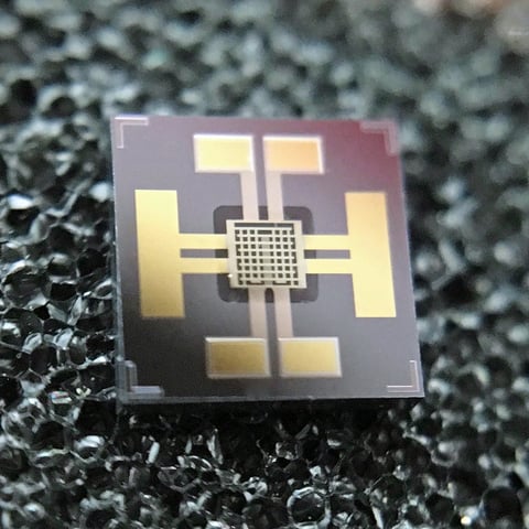
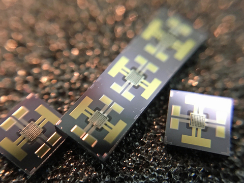
Reflective of the market demand, Micralyne observed a growing demand from its customers for standard building blocks for miniaturized gas sensors. To better support customers, Micralyne has extended its process and platform offerings to include support for extremely miniature low-power gas sensing structures. Metal Oxide Gas Sensor with integrated micro hotplates as small as 1 x 1 mm are possible on the new platform (figure 1).

Silicon Nitride and Tin Dioxide layers are transparent.
Operating characteristics of MOS gas sensors are dominated by surface reactions at the metal oxide surface. The change in resistance of the MOS material caused by the target gas can be measured with a simple voltage divider circuit and a reference resistor. Micralyne’s platform offers numerous options for the Metal Oxide films that can be used as sensing layer, including SnO2, TiO2, ZnO, In2O3, and carbon nanostructured films. The sensing layer can contain catalyst doping of Pd, Pt, or other metal oxides for increased sensitivity. Additionally, grain structure and surface area can be controlled to maximize sensing performance.
The platform includes an Electrode structure to connect the Sensor Layer to the circuit. Alternate options for metallization are available - typically Au, Al, or Pt metallization. The platform also includes an integrated micro heater within the die that can be heated to optimum sensing temperatures ranging from 200°C to 400°C. Thermal isolation is accomplished through a suspended dielectric membrane with the underlying silicon removed.
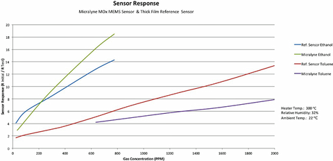
The sensing response of the Micralyne MOS MEMS Sensor was compared with conventional thick-film sensors. The MEMS version achieved similar sensitivity as the larger thick film device with an initial resistance to test resistance ratio of 18:1 at 800 ppm (parts per million) of ethanol in air with 32% Relative Humidity (figure 2). As with all MOS sensors, relative humidity must be considered since this factor will also affect sensor resistance. The MEMS sensor was also able to detect toluene in the range of 600 to 2000 ppm with an initial resistance to test resistance ratio as high as 8:1. The response time of the MEMS sensors is well below one second. The MEMS device returns to higher resistance roughly twice as fast as the conventional sensor upon removal of the analyte from the gas flow.

Micralyne’s MEMS MOS platform enables the fast development of commercial gas sensors that are low-power and extremely miniaturized for consumer and IoT markets. These sensors can enable quantification of localized environmental air quality which is critical for monitoring real-time air conditions at the individual level. Sensitivity of MOS devices is dependent on the selection of materials and operating parameters.

These characteristics can lead to increased selectivity of gas species using multiple sensor membranes integrated on a single chip. The Micralyne platform offers numerous choices for gas sensor designers depending on the gas type, concentration range, and cost considerations of their application. These devices can be easily packaged in chip-scale-packages with ASICs for device control plus additional functionality such as wireless connectivity.
About the authors
Paul Pickering
VP of Business Development and Chief Revenue Officer
Micralyne Inc.
Edmonton, Alberta, Canada
Mr. Pickering has worked more than 35 years in semiconductor and micro-fabrication technology companies with a specific focus on Medical and Bio MEMS applications for the last 5 years. He is currently overseeing the Product Marketing and Business Development teams for Micralyne Inc based in Edmonton Alberta, Canada. During his career, he has held various product line executive roles in large semiconductor manufacturers as well as several start-up companies. He co-founded two venture backed companies and has consulted with numerous other start-up companies. Prior to joining Micralyne, he served as the Executive VP, Sales and Marketing at Exar Corporation an analog and mixed signal semiconductor manufacturer. He is a graduate of West Chester University of Pennsylvania and also attended Widener University in Chester Pennsylvania.
Shailja Tewari, BASc (CE), MBA
Chief Marketing Officer
Micralyne Inc.
Edmonton, Alberta, Canada
Shailja is a global and international marketing and product management executive with extensive experience in several industrial verticals – Semiconductors, IT, Medical Devices, and Clinical and Preclinical Imaging. Shailja is passionate about the intersection of technology, engineering, healthcare and business and has been responsible for leading roadmap; product development and successful product launch strategies for numerous innovative products globally.
Shailja has a Masters of Business Administration—Rotman School of Management, University of Toronto and Bachelor of Applied Science and Engineering, Computer Engineering - University of Toronto. She is affiliated with several mentoring programs for Women in Engineering and Technology, as well as Entrepreneurship and Business.
Collin Twanow, M.Eng, P. Eng
Vice President of Technology
Collin has worked at Micralyne for more than 15 years and is currently the Vice President of Technology. Previous roles have included Vice President of Engineering, Vice President of Sales and Business Development, Director of R&D, Product Line Manager for Optical MEMS, R&D Project Manager, and Development Engineer. He is primarily responsible for Micralyne’s technology development roadmap. He is also responsible for technical problem solving and communicating Micralyne’s capabilities to the MEMS market.
Collin has managed development programs for many devices including optical telecom switches, silicon optical bench, implantable medical devices, MEMS microphones, pressure sensors, and components for military applications. Throughout these projects, he has gained extensive experience in wafer processing, design layout, device test, and failure analysis.
Collin is a Professional Engineer and holds a B.Sc in Engineering Physics (1997) as well as a Master’s of Electrical Engineering degree with a specialization in Microfabrication (2002). Collin has also lectured on microfabrication topics at the University of Alberta.