
Nanusens claims its CMOS nano-sensor technology successfully solves the stiction problem in Micro ElectroMechanical Systems (MEMS) inertial sensors, reportedly a major source of failure for this type of sensor. The problem of stiction is caused by attractive forces that occur on microscopic levels such as Van der Waals and Casimir. These are surface-area dependent and not mass dependent.
In an inertial sensor design, there is a proof mass connected to a spring. This mass moves when there is acceleration and movement is detected by the mass acting as one electrode and the change in capacitance is measured relative to a second fixed electrode. However, if there is a large movement such as from a shock or collision, the mass goes beyond the normal range of travelling and touches a surface enclosing the sensor where it 'sticks' due to the attractive forces and stops working. This can be countered by having stronger springs but this reduces the sensitivity of the sensor. A solution to increase the sensitivity could be to increase the mass but this results in a greater surface area for the mass and so, unfortunately, more attractive forces.
The approach used by Nanusens is to reduce the sensor design by an order of magnitude from Micro ElectroMechanical Systems (MEMS) with linear feature sizes of 1-2um to Nano ElectroMechanical Systems (NEMS) where the features are 0.3um. This reduces the attractive forces significantly as the surface area reduction is in two dimensions, i.e. almost two orders of magnitude reduction. Reducing the proof mass could result in decreased sensitivity except this is offset by reducing the gap between it and the fixed electrode. The size reduction also means that the energy stored on the proof mass when it hits the surface in case of a shock, it is much less and the travelling gap is also small. A shock with less energy is also easier to detach.
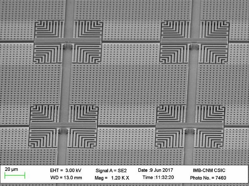
The unique nano-sensors are made using standard CMOS processes and mask techniques. The Inter Metal Dielectric (IMD) is etched away through the pad openings in the passivation layer using vapour HF (vHF) to create the nano-sensor structures. The holes are then sealed and the chip packaged as necessary. As only standard CMOS processes are used, and the sensors can be directly integrated with active circuitry as required, the sensors can potentially have high yields similar to CMOS devices. More details about Nanusens and its developments are available online.