

In little more than half a century the semiconductor industry has become the enabling factor of modern life. Undoubtedly it stands on the shoulders of giants, to paraphrase Sir Isaac Newton, but it continues to advance at an amazing pace; each new technology node brings greater transistor density and with that comes smaller integrated devices. Modern electronic devices directly benefit from this trend, with each new generation of smart phone, computer or other portable device managing to add more functionality in to ever smaller form factors.
The proliferation of wireless connectivity is a more recent but no less significant development, while MEMS technology continues to revolutionize sensor development. Together these trends lie at the heart of perhaps the biggest mega-trend of all; the Internet of Things (IoT). Much more than just a buzzword or a new way to describe existing applications, the IoT is creating new applications and new markets, along with new industry sectors to address those markets.
Estimates for the size of the IoT within the next five years vary but some industry analysts put it as high as 50 billion devices. Many will be sensor nodes; relatively small and inexpensive devices intended to be deployed liberally, most likely connected to a wireless gateway of some kind and expected to operate for many years on a single cell.
Despite needing to be ultra-low cost these nodes will, nevertheless, feature some of the most advanced integrated technology yet developed. They will invariably be based on an ultra-low power microcontroller (MCU), coupled to one or multiple sensors; increasingly a single MEMS sensor module will comprise multiple functions such as an accelerometer, magnetometer and gyroscope. Such nodes may be static or attached to assets for tracking purposes, in truth the possible applications are limited only by the imagination and the ability to manufacture the nodes cost-effectively.
Next page
Making More Of Moore's Law
High volume manufacturing is what the semiconductor industry is good at; it has to be, because the rate at which the average selling price for integrated devices falls is almost the same as the rate at which transistor integration rises. Both can be seen as aspects of Moore's Law.
In order to take full advantage of Moore's Law at the PCB level, component packaging technology is also developing. The emergence of wafer level chip-scale packaging has produced devices measuring barely more than the die itself, with ball grid array pitches of just 0.4 mm. Components using advanced packaging may measure less than 3 mm on each side and under 1 mm high, yet integrate all the functionality of a sophisticated sensor hub.
While the semiconductor industry will include multiple test stages as the components are fabricated, diced and packaged, it is still necessary to perform final tests on the products they enable. Typically, the volumes will be much lower at this point and so amortizing the cost of test across the number of products will be more difficult. Design for Test is therefore not only good engineering practice but it is essential from a commercial perspective; the speed of final test has to be optimized if budgets are to be met. This is particularly true for any OEM developing and manufacturing low-cost IoT nodes.
With packaging now so small and access to the component's pads so difficult, physically accessing test points on a populated PCB is becoming increasingly difficult, particularly on multilayer PCBs that may also use buried vias. Restricted physical access to nets makes it much more challenging to achieve good test coverage using some production test methods, such as a bed-of-nails, flying probes and in-circuit testing – all of which are used in volume manufacturing because of their speed and throughput. Limited node access becomes even more apparent with modern MEMS-based sensors due to their packaging and size.
Fortunately the semiconductor industry foresaw this problem over twenty years ago and developed Boundary Scan. Since 1990, Boundary Scan has seen continued adoption by semiconductor manufacturers. Often the Boundary Scan interface is used for in-circuit emulation, debug or programming, but in reality it offers much more than this. Using Boundary Scan it is possible to test anything from a single component to an entire PCB, through one simple interface at any stage of production; even before the firmware has been loaded (see figure 1).
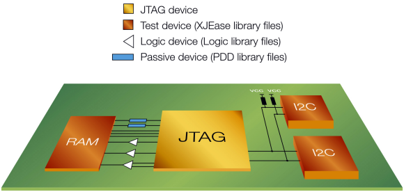
Fig. 1: Boundary Scan enables electrical access to physically inaccessible parts of a circuit.
Now commonly referred to as JTAG – which stands for Joint Test Access Group – it is a family of standards (IEEE 1149.x) that defines the physical and functional features inside an integrated device, along with the software interface. Depending on how the IC manufacturer implements it, Boundary Scan can provide access to all of a device's functional pins through a five-pin port (although a two-pin version is also available).
As the JTAG port is often accessed using GPIO instead of dedicated pins, Boundary Scan/JTAG can be supported in even the smallest of devices. The LPC81xM from NXP is a family of 32-bit ARM Cortex-M0+ based MCUs with a host of features and interfaces, and in its 16-pin XSON16 package (small-outline no leads) it measures just 3.5 mm by 3.14 mm. Its small size makes it well suited to sensor fusion applications in the IoT, however as an SMT package with a pad pitch of 0.4 mm and pad width of just 0.22 mm, physically accessing its pads for test purposes can be a challenge. Despite having just 16 pins, however, the LPC812M101JTB16 still supports the 5-pin version of JTAG. This means that, using Boundary Scan, it can be used as a 'gateway' in to an entire circuit for test purposes.
Coupled to a MEMS sensor module, such as the LSM330 iNEMO inertial module from STMicroelectronics, the LPC812M101JTB16 can easily provide the functionality of a sensor node for an IoT application. The ST module is packaged in a 24-pin Land Grid Array (LGA) package measuring 3.5 mm x 3.1 mm, yet integrates a 3D accelerometer and a 3D gyroscope, and is able to provide six dimensions of orientation detection.
Next page
Extending Boundary Scan
Testing sensor nodes in a volume production environment is a typical application for Boundary Scan. Once configured, testing would check for open- or short-circuits on all accessible nets, as well as stuck-at faults or missing pull-up/down resistors. These tests are the default for systems like XJTAG's and can be executed with the minimum of configuration; once the netlist and BOM have been imported and the Boundary Scan Description Language (BSDL) files associated with any JTAG-compliant devices on the board (such as the MCU). However thanks to XJTAG's flexibility and support for custom test scripts, testing can also be extended to include non-JTAG devices such as the inertial module. An example of a sensor node based on these two devices is shown in figure 2.
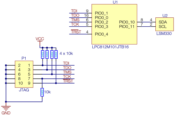
Fig. 2: A typical IoT sensor node design based on a low power MCU and MEMS sensor module.
Only JTAG-compliant devices have a BSDL file (a file that describes the Boundary Scan features it supports), but through XJTAG's software it is possible to write and execute tests at a high level of abstraction to use Boundary Scan to access any nets connected to a JTAG-compliant device. In this case, the inertial module can be accessed via the MCU over the I2C/SPI interface, using a test script that calls the protocol (provided as part of the XJTAG system) to read and write instructions/data to and from the inertial module.
The tests are written in a simple, high-level language called XJEase, which will be instantly familiar to engineers already using C or other similar language. XJTAG's integrated development environment, XJDeveloper, is supported by a free library of device-centric test models written in XJEase, and also supports the development of custom XJEase scripts to further extend test coverage. Figures 3a-c show parts of the test model developed by XJTAG specifically to functionally test ST's LSM330 iNEMO inertial module.
The LSM330 inertial module features its own self-test mode which can be initiated over I2C using the test script written in XJEase. The tests run quickly and automatically, with the results presented to the operator with a clear pass/fail indication. As an example, figure 3a shows the XJEase code used to read the LSM330's identification.
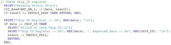
Fig. 3a: The test model first identifies the LSM330 before testing.
Once validated, the self-test mode is initiated and the accelerometer's register is read (figure 3b).
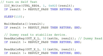
Fig. 3b: After initiating the self-test mode, the test model reads the value of the accelerometer.
Following that, the gyroscope's functionality is tested (figure 3c), while at every stage the results of the tests are relayed to the test engineer's screen.
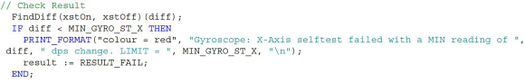
Fig. 3c: Reporting the status of the gyroscope to the test engineer is simple using XJEase.
XJTAG provides a number of tools for developing and executing tests, tailored to the needs of product developers, test engineers and a production environment, but all of the test models are developed using XJEase and will run in all of XJTAG's software products. The device under test is connected using the JTAG Controller, XJLINK2. Once connected and with the software installed on a PC, the engineer is able to rapidly configure the system, initiate tests and get direct on-screen feedback of the results.
The challenge of meeting the expectations of the IoT are becoming clear; 50 billion devices in five years equates to almost 200 million per week, or put another way more than 25 million new devices coming online every single day. Meeting that level of output, even for small sensor nodes, will require an unprecedented increase in manufacturing and testing efficiency. Boundary Scan can help meet that challenge by delivering greater test coverage in the IoT.
XJTAG Demo: http://www.xjtag.com/jtag-testing/xjtag-evaluation.php
About the Author
Philip Ling is the Technical Marketing Manager for XJTAG. He has worked in the electronics industry for 30 years as an engineer, journalist and marketeer, and holds a Post-Graduate Diploma in Advanced Microelectronics for Industrialists.
Related Stories
IoT Sensors Market to Reach US$34.75 bn by 2023
Semtech and ARM Introduce mbed IoT Device Platform for LoRaWAN Specification