
Hall effect sensors have been used to measure electric current for many years. Because of their relatively low sensitivity, conventional Hall sensors need magnetic circuits that serve to increase their cost, size, and weight. The Hall effect current sensor presented in this article features an integrated magnetic concentrator (IMC) that boosts its sensitivity enough to measure current directly, without a ferrite core.
Configuration and Operation
The IMC Hall effect sensor is fabricated by means of standard CMOS technology, with an additional ferromagnetic layer characterized by high permeability and low coercive field (very soft) bonded to the chip surface (see Figure 1).
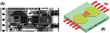 Figure 1. An X-ray of the IMC Hall sensor (A) shows the integrated magnetic concentrators placed over the CMOS Hall elements. The horizontal magnetic field is converted to a vertical field near the Hall elements (B). |
This layer functions as a magnetic flux concentrator; it provides additional magnetic gain of ~10, increasing the output signal without doing the same to the inherent sensor noise. Another distinction is that the IMC Hall sensor responds to a magnetic field parallel to the chip surface, whereas a conventional Hall sensor detects a field perpendicular to its surface (see Figure 2).
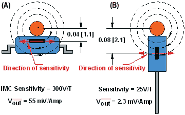 Figure 2. By comparing a typical linear Hall sensor with the IMC Hall technology, it can be seen that the IMC has sensitivity parallel to the surface and can be positioned close to the conductor (A). The conventional Hall sensor has sensitivity perpendicular to the surface; because of the package size, it cannot be mounted near the conductor (B). |
IMC sensors are also more sensitive than conventional Hall technology, making them similar to magnetoresistive sensors but without the associated drawbacks such as nonlinearity, hysteresis, and insensitivity to field direction.
|
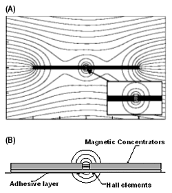
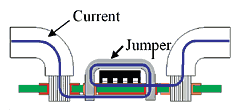
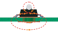
The ferromagnetic layer is structured so that a narrow gap is created in the approximate middle of the chip, where the perpendicular component of the field is strongest (see Figure 3). The concentrator locally converts the magnetic field parallel to the chip surface into a field perpendicular to it. The two sets of Hall elements placed near the gap have reverse outputs because the field direction into one set is opposite that into the other set. Their outputs are summed together to enhance the SNR and also to make the device insensitive to fields perpendicular to the chip surface. The result is a sensitivity of 300 V/T (30 mV/G). Furthermore, because the sensor is sensitive to fields parallel to its surface, it is ideal for measuring current in conductors above or below itself.
How Hall Effect Sensors Measure Current
|
| (1) |
In a vacuum (or air), the magnetic induction (or flux density) B can be calculated from H by multiplication with the permeability:
| (2) |
| If, |
then 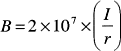 |
(3) |
where:
| B | = | flux density (teslas) |
| I | = | current in conductor (amps) |
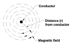
| r | = | distance (meters) |
For example, flux density at a distance r = 2 mm from a current conductor carrying
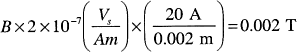 |
(4) |
With the IMC Hall sensor?s sensitivity of 300 V/T,
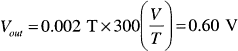 |
(5) |
The IMC Sensor at Work
Because the magnetic field strength drops off very sharply with distance, the closer the sensor can be placed to the conductor, the higher the output voltage. IMC sensors? sensitivity to fields parallel to the package surface allows the conductor to be positioned very close to the sensing element. This feature, and a sensitivity ~10 × that of conventional Hall devices, provide an output ~20 × greater than that of standard Hall sensors.
For instance, the IMC sensor can be mounted on a PCB to measure the current in traces directly under the IC (see Figure 5).
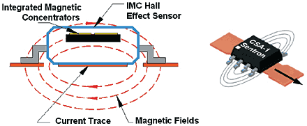 Figure 5. With an SOIC-8 package and sensitivity parallel to the surface, the IMC Hall effect sensor is ideal for measuring currents in traces on a PCB. |
Bidirectional output allows the sensor to measure both AC and DC currents. The only coupling between the IC and the conductor is a magnetic field; the sensor is thus completely isolated from the conductor and no optical isolators are required.
Because the upper limit of the current an IMC sensor can measure is determined by the maximum field, larger currents can be handled by simply moving the conductor farther away from the sensor. With a trace directly under the IC, the optimum current for the sensor is 10?20 A. To handle higher levels of current, multiple layers of copper traces can be incorporated in the PCB trace to distribute the current density and thereby increase the total current capability. The differential output voltage for this configuration can be approximated by:
| (6) |
|
|
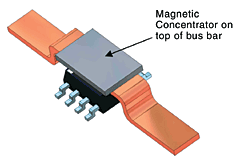
High currents can be measured by placing a formed copper bus bar over the IC. The standoff distance and size will depend on the full-scale output desired. An approximation of differential output voltage can be obtained with:
then 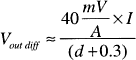 |
(7) |
where:
| d | = | distance (mm) between conductor center and sensor surface |
| I | = | current (amps) in conductor |
For example, if I = ±80 A and d = 1 mm, then:
| then |
(8) |
|
Another way to measure high currents on PCBs is to use a large, thick-gauge copper trace capable of carrying the higher currents on the opposite side of the PCB. An advantage of this configuration is that the PCB material provides additional electrical isolation between the sensor and the current-carrying conductor. The sensor should be located near the center of the trace.
Typical Applications
Among the potential applications for surface-mount current sensors are motor control, overload sensing, fault detection, current present detection, phase monitoring, PWM controllers, DC/DC converters, diagnostics, and instrumentation.
Summary
IMC Hall effect technology provides a unique solution to current sensing by combining all the advantages of Hall sensors, such as high linearity and low hysteresis, with the high sensitivity found in magnetoresistive devices. Packaged in a small 8-pin SMD, the technology lends itself in particular to applications where space and weight are a concern. Although this article has focused on current sensing, which is the primary use for these devices, they are good choices for other areas as well, including magnetic field measurement and long-range proximity sensing.