
In an image- and video-centric world, the ability to see and record images and motion accurately in full 3-D is a constant quest. This crusade for higher-resolution 3-D is driven by the expanding demand for enhanced computer vision capabilities from professionals and consumers alike, which together translates into an extremely large market. Stepping up to meet those demands,
Qualcomm and Himax Technologies are collaborating to develop and commercialize a high-resolution, low-power active 3D depth sensing camera system. The team effort will pair Qualcomm’s Spectra technologies, computer vision architecture, and algorithms with Himax's wafer-optics technology and sensing, driver, and module integration expertise. The end result is the Structured Light Module (SLiM), a 3D camera module capable of accurate, real-time high-res depth sensing and 3D point cloud generation. It boasts equally high performance in both indoor and outdoor environments. The SLiM camera module is expected to be highly desirable for use in applications that include biometric face authentication, 3D reconstruction, and scene perception in various mobile, IoT, surveillance, automotive, and AR/VR components.
What Is Spectra Technology
In their second-generation, Qualcomm Spectra image signal processor (ISP) family employs a hardware and software architecture designed to support advancements in computer vision, image quality, and power efficiency in future versions of the company’s Snapdragon platforms. It features multi-frame noise reduction to boost photographic quality, hardware-accelerated motion compensated temporal filtering (MCTF), and inline electronic image stabilization (EIS) for camcorder-like video quality
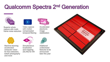
Providing low-power, high-performance motion tracking capabilities, the ISPs rely on simultaneous localization and mapping (SLAM) algorithms to support extended reality (XR) use cases for virtual and augmented reality applications that require SLAM.
Wafer Level Optics
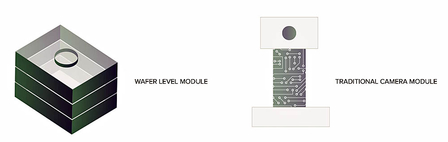
Simply put, wafer level optics is a technique whereby optical functions are manufactured onto silicon using semiconductor processes on wafers. Himax wafer-level optic devices contain camera lenses for use in portable designs. The features and advantages of these devices for engineers and designers include high-temperature availability, standard parts exhibit a smaller size in x, y, and z axes, multi options for assembling with PCB, and easy assembly.
Structured Light Module (SLiM)
Stated earlier, the Structured Light Module (SLiM) is a collaboration that brings together Qualcomm Spectra technologies and Himax's complementary technologies in wafer optics. The turn-key 3D camera module is expected to be a game changing technology for smartphones, where the companies will enable the Android ecosystem to provide the next generation of mobile user experience, according to Jordan Wu, President and Chief Executive Officer of Himax Technologies.
Qualcomm and Himax will commercialize the SLiM 3D camera as a total camera system for a wide array of markets and industries with mass production slated for the first quarter of 2018. For more details visit the Qualcomm and Himax websites.