
Over the past 20 years, the microelectromechanical systems (MEMS) sensor industry has made continuous improvements. A few years ago, for example, Motorola integrated additional signal conditioning with the sensing element [1,2,3]. Most recently, the company redesigned its line of integrated pressure sensors with onchip compensation and amplification. The company’s latest MEMS sensors feature new transducer and circuit design, process revisions, and improved packaging technology, which translates to improved performance and greater flexibility for users.
Optimizing Performance
Simplification of the photolithographic masking steps and/or process geometries can enhance throughput, product availability, and delivery. The reduced diaphragm size and simpler integral signal-conditioning circuitry of these pressure sensors result in an overall area reduction of ~30%. Reducing the die size inherently improves quality because it lessens the possibility of a critical defect’s occurring on any individual chip. The cost is lower, too, because an increased number of units are available from a given wafer size. The reduced die size also allows the die to be used in smaller packages (see Photo 1 and Table 1). The improvements noted in the table are the result of revisions to the manufacturing process and improvements in transducer design and circuit design, temperature calibration, and processing [4].
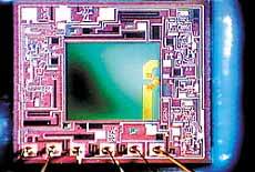
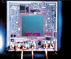
Photo 1. A photomicrograph comparison of the old 120 by 120 mil layout (A) and new 105 by 105 mil size (B) of the 100 kPa die shows the smaller footprint of both diaphragm and circuitry.
Process Revisions
The wafer fabrication process for both the original and redesigned pressure sensor combines conventional bipolar IC technology with bulk micromachining. This proc ess etches away most of the thickness of a region of the die, called the diaphragm. The bipolar process provides the diffusion for the piezoresistive (stress sensing) transducer, and also provides the process flow for the op amps. One area of the diaphragm concentrates mechanical pressure stresses, increasing them to measurable levels.
c (3.05 mm by 3.05 mm) (2.67 mm by 2.76 mm) c sink/source capability, simpler to trim etch stop thickness controlTABLE 1 c Old Design New Design Improvements Noted Die size 0.120 in. by 0.120 in. 0.105 in. by 0.105 in. Increased die/wafer Circuit 3 op amp 2 op amp More robust design, adds Transducer X-ducer Picture frame Higher sensitivity Etch technique Timed Electrochemical Tighter diaphragm Trim at temperature Reverse bias Onchip heater Tighter Tc performance
The etching process used to create the thin (typically <0.001 in. thick) diaphragm makes the silicon wafers more fragile and susceptible to breakage during handling. To reduce in-process damage, Motorola performs the etch process as the last major photolithography step. Once the sensors are separated from the wafer and packaged, the diaphragm is actually quite rugged, tolerating overpressure several times the device rating. Burst pressure is typically several times the rated pressure; as an example, the MPX5100 has a rated pressure of 100 kPa and a minimum diaphragm burst strength of 1000 kPa (140 psi). 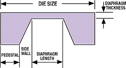
Figure 1. In this cross section of a typical piezoresistive pressure sensor, the angle of the side wall is a highly reproducible (54.7°) feature of anisotropic bulk micromachining because it follows the crystal structure. Reducing the diaphragm length and the circuitry area (on the solid portion of die) yielded a smaller die size.
Motorola also changed the silicon etch process used to create the diaphragm from a timed etch to an electrochemical etch-stop (ECE) technique. In general, a timed etch is controlled by etch time, temperature, and etchant (KOH, potassium hydroxide) concentration. The etching process is terminated when the wafer is removed from the etch tank. The timed etch process is easy to implement and does not require additional semiconductor processing or special design modifications. It does, however, produce large thickness variations for diaphragms across a wafer and from one wafer to another.
In its favor, the ECE technique allows tighter control of the diaphragm thickness and more predictable distribution, which results in a narrower range of device parameters to be calibrated. The etch-stop technique uses a p-type substrate with an n-epi layer, tightly specified for thickness and resistivity. During etching, the wafer is immersed in the KOH bath, and a controlled bias is applied between the n-epi layer of the wafer and the etch bath, making the p-n junction act as a reverse-biased diode. In the reverse-biased mode, the diode prevents the etchant from being exposed to any current, and the KOH performs a normal anisotropic etch through the substrate until it reaches the junction. Then, because the diode has been etched away, the KOH is exposed to the applied bias, and a reaction forms a thin layer of silicon dioxide that stops the etch. The diaphragm thickness is therefore unaffected by typical variations that affect the timed etch; instead, it is necessary only to ensure that the wafer is supplied with the correct n-epi thickness, junction bias voltage, and bath temperature.
Tighter control of diaphragm thickness permits a reduction in both thickness and width which, combined with the decreased area for the circuitry, reduces the overall die dimensions from 120 by 120 mil to 105 by 105 mil for the typical 100 kPa sensor. Other pressure ranges are reduced in size by similar percentages.
Transducer Design 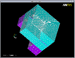
Figure 2. Finite element analysis of a typical 100 kPa absolute pressure sensor provides a quarter-symmetry model of the sensor with constraint and die bond. A very fine mesh size was used near the transducer location at the edge of the diaphragm (yellow circle).
Parameters for the mechanical design of the sensor include diaphragm thickness and width and transducer placement. The goal of this design was to achieve a high level of sensitivity, while using a compact dia phragm to ensure a low linearity error. Several design and process changes allow the use of a smaller die and increased accuracy. For example, a reduction in typical diaphragm thickness from 24 to 18 mm allowed the use of a smaller diaphragm because element sensitivity scales as the ratio of diaphragm length to thickness (L/t). A 25% reduction in thickness therefore allows a 25% reduction in diaphragm width and, as a result, 36% less diaphragm area (see Figure 1). As previously noted, the use of ECE facilitates the manufacture of thinner diaphragms.
Finite element analysis was used to model candidate designs and to find the optimum diaphragm width and transducer placement (see Figure 2). With this modeling technique the mechanical design was completed in one iteration. It took into account the silicon, surface oxide, and nitride layers; the elastomer die bond; and the glass frit constraint adhesive, when applicable. (Absolute pressure sensors require a reference cavity sealed with glass frit adhesive, but differential devices do not.) Mechanical stress values were converted to transducer output voltages using piezoresistive theory [5], and these voltages were then used in circuit models to simulate the performance of the entire sensor. 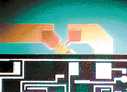

Photo 2. The earlier single-element X-ducer piezoresistor (A) can be contrasted to the new single-element picture-frame design (B).
A more efficient transducer was used to produce a larger electrical signal from the same level of mechanical stress. Motorola’s original design was the X-ducer sensor, a single diffused element shaped like an X (see Photo 2A). This design provided a tight offset distribution as compared to the Wheatstone bridge designs used in most of the first micromachined pressure sensors. Improvements in processing and design, however, made a tight offset distribution possible without using the X-ducer design. As a result, Motorola developed the picture-frame design (see Photo 2B), which provides ~40% more span than did the X-ducer. Increased efficiency yields both better linearity and a higher SNR. The improved output signal allows a lower overall gain to be used, enhancing system accuracy.
In addition to test data, test chips were made without signal conditioning circuitry. These “transducer-only” test dies allowed both direct measurement of transducer performance and validation of mechanical and transducer models. The new design was verified using a combination of transducer test data, modeling, and circuit models.
Circuit Design
To meet the target specifications, Motorola used a simpler circuit with one fewer stage in the amplification circuitry than called for in the earlier design [6]. With fewer resistors (see Figure 3), the circuit is easier to calibrate during a laser trim process. In addition, a source or sink can be obtained in the new design. Motorola designed the output stage to drive a CMOS A/D input from 0.2 to 4.7 V (typical values) with a 5 V supply voltage.
Both sensor designs use laser-trimmed thin film resistors to calibrate sensor output. Many of the resistors shown in Figure 3 are chrome silicide (CrSi), adjusted with partial cuts during laser trim. Trimming allows parameters such as sensitivity, zero pressure offset, and temperature response to be adjusted. Motorola’s revised laser trim algorithm, with basic principles similar to those of the earlier
version, offers several important improvements. A balanced design enables bidirectional trimming of all parameters and more independent trimming of each parameter. On the original circuit, certain parameters could be trimmed in one direction only. If processing variations resulted in the initial value of those parameters’ being beyond the target values, the device could not be properly calibrated. Additionally, many parameters had to be handled in an iterative process in which several parameters were roughly trimmed, then all trimmed again to reach the final target. Any adjustment of one resistor affected more than one parameter, however, and limited the overall system accuracy. On the new design, all parameters can be trimmed in either direction, and each one is measured and trimmed independently of the others. This new circuit provides both more accurate trim capability and reduced trim time.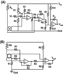
Figure 3. A circuit comparison of the original three op amp design (A) and the new two op amp design (B) reveals the reduced component count in the latter.
The reduction in onchip compensation circuitry also permits the incorporation of an onchip heater used during the temperature coefficient of offset (Tco) trim. Because Tco is influenced by both the wafer and assembly processes, an active Tco trim is performed by heating the device, measuring Tco, and then making the appropriate compensation. Several methods, including dedicated equipment with external heating, can be used to heat the device, although the step is expensive and time consuming. The original Motorola circuit used a reverse-biased diode to heat the die, and then switched back to a forward bias to measure the Tco and trim the device accordingly (see Figure 4A). The new device has an onchip heater that is controlled independently from the rest of the circuit. During Tco trim, the heater is turned on and a controlled voltage wave form is applied, so that the die is heated and rapidly reaches a steady-state temperature. The Tco is meas ured and compensated, and then the heater is deactivated (see Figure 4B).
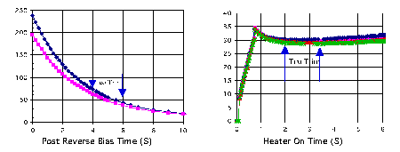
Figure 4. Either reverse bias (A) or an onchip heater (B) can be used for trimming the temperature coefficient of offset (Tco). As shown by the temperature D (the temperature difference between chip and ambient) vs. time plots for the two methods, the reverse-bias method heats the die initially but then turns the power off and must trim the die during cool down. The onchip heater allows steady heating during trim, providing better temperature control.
Packaging Alternatives
Packaging is a major challenge for MEMS technology. Most pressure sensors, for instance, must be directly exposed to the measured fluid, but most standard IC packages encapsulate the die in thermoset plastic. Packaging and mounting techniques for the sensor must provide:
• Mechanical support
• Electrical interface
• Environmental protection
• Media interface free of fluid leaks
• Mechanical stress isolation
• A low-cost, small packaging solution compatible with standard manufacturing processes
The ~30% reduction in die size allows the entire Motorola integrated pressure sensor line (ranging from 4 to 1000 kPa) to be used in new, smaller packages (see Table 2 and Photo 3). Motorola’s small-outline package (SOP) offers both surface mount and throughhole options, with about half the footprint and volume of the older unibody package. The SOP is also compatible with other Motorola sensor families, such as uncompensated and compensated pressure sensors.
The leads of the SOP are designed with standard 1/27 mm wide/40 mil spacing and 2.54 mm/100 mil pitch. The solder-bond pad sizes and solder paste application are the same as for other semiconductor components, and the lead surface finish (copper with nickel and gold plating) is compatible with most soldering operations. c cTABLE 2 Package Body size Overall footprint Features unibody 0.700 in. dia. 0.700 in. by 0.810 in. Proven throughhole design. Next generaton 0.546 in. by 0.663 in. 0.546 in. by 0.868 in. Allows surface or throughhole mounting options. small outline package (SOP) 0.420 in. by 0.420 in. 0.420 in. by 0.715 in. Allows surface mount or through-hole options, small footprint.
TABLE 3 Characteristic Minimum Typical Maximum Unit Differential pressure range 0 c 100 kPa Full-scale output 4.487 4.7 4.813 V Zero pressure offset 0.088 0.2 0.313 V Overall accuracy –1.5 c 1.5 % F.S. span Linearity c 0.3 c % F.S. span
Next-Generation Performance 
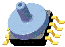
Photo 3. The small-outline package surface mount pressure sensor packages are shown without port (A) and with pressure port (B).
The key parameters for a 100 kPa integrated sensor are shown in Table 3 [7]. With the smaller die size, smaller dia phragm, and simpler circuitry, this device provides an accurate, compact, and inexpensive pressure measurement that is compatible with standard MCUs. This perform ance level has been successfully demonstrated for a number of high-volume, sensitive applications, including:
• Industrial—altimeter, load leveling, and level detection
• Medical—personal blood pressure meters and hospital beds
• Engine management—manifold or barometric absolute pressure
The range of pressures that can be addressed by the new integrated sensor has been extended. On the low side, improvements in process and design allow more accurate measurement of low pressures. As a result, a fully integrated 4 kPa differential device is now available. Packaging and test capabilities remain limitations to the higher pressure ranges, especially for sensors offered in high-volume, plastic-molded packages.
Motorola plans to extend this new die design to the entire integrated pressure sensor line (4–1000 kPa) and provide new packaging options. To make other MEMS devices economically viable, Motorola will be taking many of the same steps that improved the performance and reduced the cost of its integrated pressure sensor.
Acknowledgment
The authors thank Stephen Lin for his contribution to the design and process changes that made the next-generation sensor possible, and Bill McDonald and Dan Wallace for their contribution to the SOP design.
X-ducer is a trademark of Motorola Inc.
References
1. I. Baskett et al. 1991. “The Design of a Monolithic, Signal Conditioned Pressure Sensor,” Proc Custom Integrated Circuits Conference, IEEE 27.3:1-4.
2. M. Shaw et al. 1998. “System Aspects of a Sensor System on a Chip,” Proc Sensors Expo Chicago.
3. Rajan Verma et al. 1997. “A Monolithic Integrated Solution for MAP Applications,” Proc SAE International Congress & Exposition, Detroit, Paper 970608.
4. R. Frank and W. McCulley. 1985. “An Update on the Integration of Silicon Pressure Sensors,” Proc Wescon/85, Integrated Sensor Technology Session Record 27, San Francisco, 27/4-1-27/4-5.
5. D. A. Bittle et al. Sept. 1991. “Piezoresistive Stress Sensors for Structural Analysis of Electronic Packages,” J Electronic Packaging, Vol. 113.
6. W.S. Czarnocki and J.P. Schuster. 1995. “Robust, Modular, Integrated Pressure Sensor,” Proc 7th Intl Cong on Sensors, Nuremberg, Germany.
7. Motorola Inc. 1998. Motorola Sensor Device Data/Handbook, Rev. 4.