Industrial IoT has created a bottleneck that threatens to overwhelm data analysis tools. Part Two of “Industrial IoT’s Smart Shift to the Edge” examines how breakthroughs in technologies make edge node processing possible.
Onward
Data sensed, measured and analyzed in an industrial setting garners valuable insights into production, safety and efficiency. The information secured by sensors leads to better business decisions and gives companies a marketplace advantage. However, to truly make an exponential positive impact data must be analyzed in real-time or the insights revealed by the accumulation of data loses value the more time passes.
Part one of this article explored how shifting the measurement, interpretation and transmission of data to the edge node enables industrial IoT (IIoT) to enhance physical assets and processes. In this half of the article let’s discuss the technologies that industrial IoT relies on to make intelligent nodes secure, energy efficient and easy to manage.
Dynamic Range, Notation And Precision
There are several options for the computational horsepower of the edge analytics. Many options are available for processing algorithms, from a simplistic MCU that provides limited controls, more sophisticated system on a chip (SoC) MCUs, to powerful multicore digital signal processing. The processing core size, a single- or dual-core operation, instructional RAM cache size, and fixed vs. floating-point needs are typical technical considerations. Often there is a trade-off between the power budget available on the node and the computational requirements of the application.
For digital signal processing, there are two notation format categories used to store and manipulate numeric representations of the sensor node data: fixed point and floating point. Fixed point refers to the manner in which numbers are represented with a fixed number of digits after and sometimes before the decimal point. DSPs using this method process integers such as positive and negative whole numbers using a minimum of 16 bits with 216 possible bit patterns. In comparison, floating point uses rational numbers with a minimum of 232 possible patterns3. DSP using a floating-point computation method can process a much wider range of values than fixed point with the ability to represent very large or small numbers.
Floating-point processing assures that a larger dynamic range of numbers can be represented. This is important if large sets of sensor node data are computed where the exact range may be unknown in advance of sensing. Additionally, because every new computation requires a mathematical calculation, rounding or truncating is an inherent result. This creates quantization errors, or digital signal noise, within the data. A quantization error is the difference between an ideal analog value and its digital representation, or nearest rounded value. The larger the quantization gap between these values, the more pronounced the digital noise will be. Floating-point processing yields greater precision than fixed-point processing when accuracy and precision are important to the interpreted sensor data.
Performance
Firmware designers should implement a computation application with the greatest efficiency, as the execution speed is critical. It is important to delineate the processing requirements for data interpretation to determine whether fixed or floating-point computations are better suited.
It is possible to program a fixed-point processor to perform floating-point tasks and vice-versa. However, this is inefficient and impacts processing performance and power. Fixed-point processors are best used for higher volume general-purpose applications that do not need intensive computation algorithms. Floating-point processors conversely can leverage specialized algorithms for ease of development and greater precision.
While not high in performance, the number of supported GPIO pins within the processor can provide secondary selection criteria. Direct support of the right control interface for the sensors of interest, such as SPI, I2C, SPORT, and UART, reduce system design complexity. The core processing clock speed, number of bits per execution, amount of embedded instruction RAM available for processing and memory interface speed all impact the capability of the edge node processing. Real-time clocks help time-stamp data and allow alignment of processing across multiple platforms.
Processing computational power is often defined in MIPS, the number of million instructions that can be executed within a second, or MMAC, the number of single precision floating-point or fixed-point multiply-and-accumulate 32-bit operations that can be executed in millions per second. MMAC performance values increase respectively by a factor of 2x and 4x for 16-bit and 8-bit operations3.
Security
While full security of the industrial IoT spans each and every system, transmission and data point access, microcontrollers and DSP offer internal security features. The advanced encryption standard (AES) provides added security on a wired link, such as UART/SPI, or a wireless link. In the case of wireless RF communication, AES encryption is performed prior to payload transmission via the edge node radio.
The receiving node performs the converse decryption. Electronic code block (ECB) or cipher block chaining (CBC) are typical modes of AES4. A security key of 128 bits or larger is often preferred. A true random number generator is used as part of the security computation within a processor.
Single Or Dual Core
Raw processing power will always be in demand. Efficient raw processing power is even better. Multicore MCUs and DSPs provide additional computational power for algorithms that specifically benefit from intensive parallel processing. However, the need to often process disparate data is also increasing. This has given rise to a class of multicore microcontrollers that bring together two or more cores with specific, but different, functional strengths. Commonly referred to as heterogeneous or asymmetric multicore devices, they often feature two cores with very different profiles.
An asymmetric MCU could feature both an ARM Cortex-M3 and Cortex-M0, which communicate using an interprocessor communication protocol. This allows the M3 to focus on heavy digital signal processing tasks while the M0 implements the lower intensive control aspect of an application5. The concept allows simpler tasks to be offloaded onto the smaller core. The partitioning maximizes the processing bandwidth of the more powerful M3 core for compute-intensive processing, which is at the heart of coprocessing. The intercore communication uses a shared SRAM with one processor raising an interrupt for the other to check. This alert is acknowledged when the receiving processor raises an interrupt in response.
Another benefit of heterogeneous multiple core MCUs is to overcome the speed limitations of embedded flash memory. By partitioning tasks in an asymmetric way across two small cores, the full performance of the cores can be accessed while still utilizing low cost embedded memory. The cost of implementing embedded flash often dictates the cost of an MCU, thus eliminating the bottleneck. Balancing the processor demands within the available power budget can be a key part of the industrial IoT edge sensor node design5.
Balance of Power
Many industrial IoT edge sensor nodes must operate for years on the same small form-factor battery, even when energy harvesting is possible. ULP operation will be a key parameter for these nodes, and components must be selected that minimize the real-world current consumption of the node6.
Many MCUs best suited for the industrial IoT are based on the ARM family of Cortex-M embedded processors, which are targeted for low power MCU and sensor applications7. These range from the Cortex-M0+, optimized for power efficient simpler applications, to the Cortex-M4, for complex high performance applications requiring floating-point and DSP operations. Higher processing cores can be used at the expense of low power.
The ARM CPUs provide a starting point in terms of code size, performance and efficiency. But many ultralow power capabilities are entirely up to the MCU vendor when the MCU’s actual current consumption is active or in deep sleep modes. Active current consumption can be heavily influenced by process technology choices, caching and the overall architecture of the processor. MCU sleep current and the peripheral functionality available while the CPU is sleeping are mostly influenced by the MCU’s design and architecture.
The EEMBC, an industry alliance, develops benchmarks to help system designers select the optimal processors by helping them understand the performance and energy characteristics of their systems. The ULPMark CP score reported for each device is a calculated single-number figure of merit. Scores for each of the individual benchmarks within this suite allow designers to weight and aggregate the benchmarks to suit specific application requirements8.
The power budget for the sensor edge node will directly correlate to its processing capacity. If the power budget does not agree with the processing needs of the edge node analytics, a trade-off may need to be made. Performance efficiency can impact the power efficiency of the sensor edge node. A typical power consumption metric for microcontrollers is to specify the amount of active current used per MHz of computation. As an example, for an MCU that is based upon the ARM Cortex-M3, the current can be in the tens of μA per MHz.
Duty Cycle
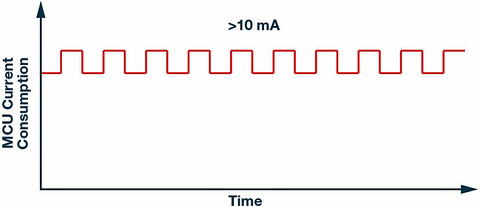
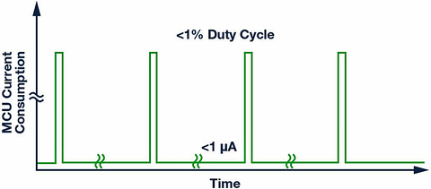
Power consumption minimization for the edge sensor node is often based on two factors: how much current the node consumes while it is active and how often it must remain active to sense, measure and interpret. This duty cycle will vary based on the type of sensor and processor used in the node as well as requirements of the algorithm.

Without consideration for the MCU current consumption, a mostly active state will consume considerable power within the edge sensor node and reduce the lifetime of a battery-powered application to mere hours or days.
Significant energy savings are achieved by duty cycling the components within the node, making sure they are active only when strictly needed. The MCU is rarely turned all the way off. It must be specifically architected for low energy operation in order to enable the MCU to keep full control of the edge sensor node while consuming as little energy as possible. Minimizing MCU current consumption is all about making the MCU sleep as often as possible while still allowing it to execute its critical tasks when they are needed.

Keeping the MCU operating within a low power hibernate mode for a mostly inactive state, only to be active during a short duty, can extend battery life for the edge node to many years.
Many edge node sensing solutions within the industrial IoT may not be required to process a continuous uninterrupted stream of data. Ignoring data from known out-of-bounds conditions using interrupt event thresholds can reduce the processing power.
To conserve both power and bandwidth, a predictable on duty cycle may be known in advance. Additionally, a variable duty cycle based on the state of sensed information can trigger either an active or reduced power state.
The response time and power consumption, both turn-on and turn-off, of the microcontroller or DSP can be important design considerations to low bandwidth applications. For example, the transmission of data from a temperature and light sensor may be reduced significantly during periods of inactivity within a building. This allows longer sleep times at the sensor node and far fewer transmissions of information.
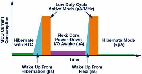
To provide a rapid reaction, many microcontrollers provide various states of low power operation in additional to being fully active such as sleep, flexi, hibernate and full power-down. Each mode will power down various internal computational blocks for power efficiency when not needed, often changing the current requirements by several orders of magnitude. The trade-off for this power benefit is that there will be some minimum finite response time to transition to full activity. In a hybrid configuration known as flexi mode, the computation core is in sleep mode while the peripheral interfaces remain active. Hibernate mode can provide SRAM data retention with the option to still allow the real-time clock to remain active.

The detailed MCU power consumption vs. timing diagram in figure 6 shows the impact of each low power MCU mode, transition time and duty cycle. Using low power states when the MCU is not active is key to keeping within a low power sensor node budget9.
Sensor Fusion
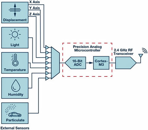
Advanced analog microcontrollers provide a full mixed-signal computational solution. A front-end analog mux with an embedded precision analog-to-digital converter (ADC) allows for a more advanced sensor fusion approach. Multiple sensor inputs can be sent to a single microcontroller ahead of digital processing. On-board digital-to-analog converters (DACs) and microcontroller feedback to other nearby equipment permits a rapid feedback loop. Other embedded circuit blocks such as a comparator, band gap reference, temperature sensor and phase-lock loop provide additional algorithm flexibility for a multi-sensor edge node10.

Analog signals from multiple sensors can be sent to a single precision analog microcontroller. Algorithms within the microcontroller intelligently can combine the information in a process known as a sensor fusion.
An example of this type of edge node processing is within an outdoor pollution monitor. In such an application, data from multiple inputs, including gas, temperature, humidity and particulate sensors, are fused and analyzed within a single processor. From this information, processing can be done to generate pollution figures based on calibration and compensation known only at the local sensor node. This calibrated data can then be sent to the cloud for historical analysis. In some cases, unique one-time commissioning may be needed to configure each sensor node for its particular environmental offsets9.
Making the Smart Shift to the Edge
Industrial IoT has moved passed the theoretical realm as businesses are incorporating sensing technology into their physical assets and daily processes. This innovation in analytics platforms to analyze the massive amount of data collected must be met with equal innovation at the hardware level to eliminate the bottleneck that threatens to overwhelm software. The smart sensor capabilities and edge node technology discussed in both parts of this article make industrial IoT not only a reality, but an efficient and secure way to command decisions about which data is relevant and provide businesses with actionable intelligence.
REFERENCES
3 Boris Lerner. “Fixed-Point vs. Floating-Point Digital Signal Processing.” EE Times, February 2007.
4 Digital Signal Processors. Analog Devices, Inc.
5 European Editors. “Multicore Microcontrollers Drive Performance.” Digi-Key, November 2013.
6 Oivind Loe. “Assessing Real-World MCU Energy Efficiency.” Embedded, October 2015.
7 Amyas Phillips. “Industrial IoT.” ARM.
8 IoT-Connect™, an EEMBC Benchmark. EEMBC.
9 Michelle Farrington. The Evolution of Self-Powered IoT Systems. IDTechEx, April 2016.
10 Precision Analog Microcontrollers. Analog Devices, Inc., July 2008.
About the author
Ian Beavers is a product engineering manager for the Automation Energy and Sensors team located at Analog Devices, Greensboro, NC. He has worked for the company since 1999. Ian has over 19 years of experience in the semiconductor industry. Ian earned a bachelor’s degree in electrical engineering from North Carolina State University and an MBA from the University of North Carolina at Greensboro.