
It’s a trend bigger than just GaN, wide bandgap semiconductors are becoming increasingly prominent in driving power conversion in AC-DC and DC-DC applications, across industrial, automotive, infrastructure and consumer worlds. GaN has very fast switching characteristics, greater power density and higher efficiency outputs than its silicon counterparts. That increase in efficiency and power density enables many benefits for consumers and enterprises alike, whether it’s a smaller form factor and a faster charging rate in consumer adapters or reductions in cooling costs and wasted energy for data centers.
Silicon-based power devices have been used for many years now but GaN devices have demonstrated the capability to displace them thanks to a combination of benefits that make them superior to their silicon counterparts:
- A low gate charge, zero reverse recovery and flat output capacitance, all of which yield a high-quality switching performance
- Higher energy efficiency
- New topologies
- The potential for lower manufacturing costs
Altogether, this produces a higher-performance successor, by many orders of magnitude, over the silicon-based MOSFETs (Metal-Oxide-Semiconductor Field-Effect Transistors).
Three Routes to Reducing GaN Costs
Emerging technologies and higher associated costs practically go hand-in-hand, and at the outset, GaN was no different in this regard. In fact, the initially higher costs of manufacturing GaN devices were a major impediment toward more widespread adoption, for both manufacturers and users. The costs involved with GaN’s wafer substrate and thicker epitaxial deposition processing have historically been the biggest factors inflating GaN’s overall bottom line.
But, this is far from set in stone. In fact, just the opposite: we can see a clear path to making improvements in the manufacturing process that can help to cut down on these expenses and bring GaN’s costs down to silicon’s level.
That path to cost parity between GaN and Super Junction MOSFET devices lies through these three routes:
- GaN HEMT (High-Electron Mobility Transistor) devices feature smaller effective areas per Rds(on) compared to their silicon counterparts. This allows for higher device density per wafer substrates, bringing down wafer costs – one of the biggest contributors to GaN’s total cost – at the same time.
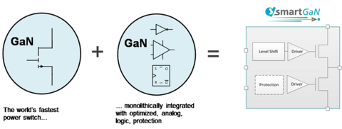
- Because of their lateral designs, GaN HEMTs also make it much easier, and more cost-effective, than silicon devices to enable a monolithic integration of multiple devices. That all helps to produce both an altogether more comprehensive solution and, consequently, a more affordable bill of material (BOM).
- Finally, a combination of more efficient manufacturing processes and reduced capital expenses (thanks to older, if not somewhat depreciated, equipment) lead to an improved epitaxial growth throughput, which, in turn, lowers overall processing costs.
Where engineers can find GaN’s real value
Developing GaN devices requires both a shift in thinking among engineers, and a shift in resource allocation. For instance, the unique structure of GaN devices enables them to drive lower gate charges, but this is only possible because of a highly tuned, or optimized, driver. It’s imperative that engineers place a premium on creating and implementing these optimized drivers to fully take advantage of GaN’s inherently faster-switching capabilities.
That’s not the only engineering advantage that GaN boasts over silicon devices. Unlike Super Junction MOSFETs, GaN devices can integrate zero-voltage switching (ZVS) controllers into their design to accomplish three goals:
- Increase switching
- Reduce heat
- Save energy
By deploying ZVS topologies, engineers stand to reduce the cost and size of magnetic parts within the GaN device, yielding further BOM savings.
For decades, silicon-based devices have been the baseline standard in the semiconductor world. In the last few years, GaN devices have made big moves in this landscape, elevated by their superior design and switching capabilities, but ultimately held back by inherently high design costs. But, not for much longer.
In 2018, we expect engineers will be able to achieve more cost-effective design measures that lower the overall BOM expenses in GaN manufacturing, to create a semiconductor device that boasts not only the best switching performance on the market, but a more mainstream-friendly price tag to go with it, too. The value in GaN is just sitting there, waiting to be unearthed – and 2018 will be the year that happens in a big way.