
For many years, sensors have incorporated an IC based on an analog sensor signal processing (ASSP) architecture. The development of fine-geometry CMOS and high-performance calculating engines, however, has recently made digital sensor signal processing (DSSP) available for use in pressure sensors. As a result, the next generation of ICs for conditioning and converting pressure transducer outputs will incorporate the DSSP architecture. Understanding the significance of what this new architecture offers requires a little background on the characteristics of MEMS pressure tranducers.
MEMS Basics
|
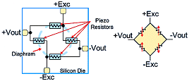
In a bridge configuration, the resistance of diagonally opposed legs varies equally and in the same direction, as a function of the mechanical deformation caused by pressure. As the resistance of one set of diagonally opposed legs increases under pressure, the resistance of the other set decreases, and vice versa. Bridge excitation in the form of voltage or current is applied across two opposite corners of the bridge. Shown as +Exc and ?Exc in Figure 1, these terminals are usually called the excitation inputs or bridge drive inputs.
| |||
Analog Sensor Signal Processing
The first generation of ICs to integrate ASSP usually included little more than differential-to-single-ended amplifiers. All of the transducer's performance peculiarities were amplified and passed on, leaving the transducer manufacturer to carry the burden of establishing sensor performance. Typically, the pressure sensor signal and temperature signal were presented to an electronic control unit, which used look-up tables to obtain a reasonable estimate of the pressure.
These architectures were used in engine management modules to process data representing barometric air pressure and manifold air pressure, and performed calibration and compensation in the analog domain. To store the sensor-specific data, such analog "memory" components as potentiometers, discrete resistors or capacitors (some of them temperature dependent), and laser- trimmed resistors were used. The major problems with this approach included:
- Restricted accuracy of compensation resulting from the sensor's nonlinearity
- High cost of laser trimmers and other automated equipment
- Multiple setups usually required for test and trim
- Miniaturization precluded by high component count
Two factors limited the performance of early designs: the use of low-resolution (8- and 10-bit) DACs and the use of a discrete temperature-sensing device connected to the signal conversion IC. The second-wave architecture was enhanced tremendously by the introduction of 12- and 16-bit DACs, and by the integration of a ratiometric temperature sensor into the IC. First order temperature compensation, in which the temperature signal is local to the IC itself, is performed entirely by the signal conversion ±C. Sensor performance was increased by 2% or more over the typical automotive operating temperature range (?40°C to 125°C), and by as much as 0.1% in industrial applications.
Digital Sensor Signal Processing
The third-generation architectural style?DSSP?is characterized by a fully digital compensation and error-correction scheme. Very fine geometry, mixed-signal CMOS IC technologies have enabled the incorporation of a sophisticated digital signal processor (DSP) into the sensor compensator IC. The DSP was designed specifically to calculate sensor compensation, enabling the sensor output to realize all the precision inherent in the transducer. Theoretically, linearizing the first and second order temperature effects on output span and offset can make the overall linearity vs. temperature better than that of the transducer itself.
As background, consider that several key factors are essential in making this third-wave architecture successful:
- Transducer repeatability over temperature and pressure
- High-resolution A/D conversions (16-bit minimum)
- Computational engine with 16-bit multiplication and addition
- Synchronous operation between digital logic and signal conversion circuits
- Ratiometric operation for all analog signal-processing subsystems
- High-resolution (12-bit) D/A converters
- Low power consumption
- Transducer stability, repeatability, and hysteresis cannot be improved by calculation.
- Calculations can degrade, but never increase the signal resolution.
- Output signal precision will be less than the input signal resolution.
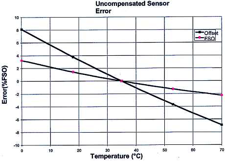 Figure 2. A slight curvature indicates second order effects in the output of this piezoresistive transducer. |
Also visible in these curves is a slight nonlinear curvature indicative of second order effects. Compensation of these temperature errors requires use of a common temperature linearization equation:
| Dout = gain (1/2 + G1 T + G2T2) (signal + Of0 + Of1 T + Of2T2) + Doff |
(1) |
where:
| Dout | = compensated output signal |
| gain | = compensates output span |
| G1 | = compensates first order gain temperature coefficient (TC) errors |
| T | = temperature (°C) |
| G2 | = compensates second order gain TC errors |
| signal | = digitized representation of uncompensated transducer signal |
| Of0 | = compensates transducer element's offset |
| Of1 | = compensates first order offset TC errors |
| Of2 | = compensates second order offset TC errors |
| Doff | = zero-pressure output level |
Evaluation of this equation requires the arithmetic operations of addition and multiplication. Though not explicitly, a third arithmetic operation (negation) is also required. To maintain the highest level of precision, all arithmetic operations should be performed at the resolution of the input signal, in this case, 16 bits.
MAX1460 Smart-ADC Architecture
A new device (MAX1460) is now available to perform the arithmetic operations required to compensate pressure sensors through the use of Equation 1. This IC includes a high-resolution, 16-bit ![]()
![]() ADC, a full 16-bit mathematical processing engine, and a fine-resolution, 12-bit DAC for signal output. Its key feature is a small and power-efficient DSP.
ADC, a full 16-bit mathematical processing engine, and a fine-resolution, 12-bit DAC for signal output. Its key feature is a small and power-efficient DSP.
The MAX1460 is an ASIC digital sensor signal processor, implemented in fine-geometry mixed-signal CMOS technology (see Figure 3).
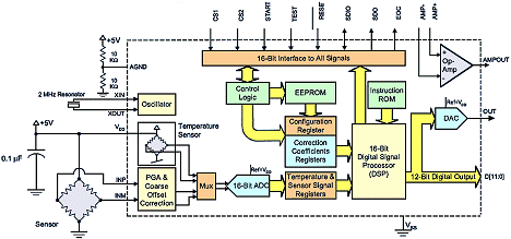 Figure 3. The MAX460 digital signal conditioner combines a 16 bit smart A/D converter with a dedicated processor and analog front end. |
It combines a 16-bit smart ADC with a dedicated processor and high-performance analog front end. Though optimized for the calibration and temperature compensation of piezoresistive pressure sensors, it offers powerful performance in applications for which the input signal is very small (millivolt range), and for which the offset and span and their temperature coefficients are in need of correction.
Calibration and compensation coefficients are stored in an internal 128-bit EEPROM. The integrated DSP then calculates the compensation correction using these coefficients, the 16-bit digitized sensor signal, and the digitized temperature data. All corrections are performed in the digital domain. The conditioned output is then presented externally as a 12-bit digital word, and (by means of the internal 12-bit DAC) as a ratiometric analog voltage proportional to the supply voltage.
The uncommitted op-amp can be used to filter the analog output or to implement a two-wire, 4?20 mA transmitter. Such built-in functionality enables the MAX1460 to support automotive, industrial, process, and aerospace applications, yielding total accuracies within ±0.5% (typical) of the sensor's inherent and repeatable error band over temperature. This residual error mainly consists of sensor nonlinearity in response to pressure and temperature nonlinearity errors higher than second order.
The MAX1460 smart ADC digitizes the sensor signal, mathematically adjusts the signal for temperature effects, and converts the result back to an analog signal (and also outputs the digital result directly). The new feature that separates this architecture from previous central processing unit circuit schemes is the presence of precision analog and digital functions on a single piece of silicon. Also integrated is the temperature measurement, which is ratiometric to the supply voltage. All is accomplished within the sensor assembly's final package, and with supply currents below those of a conventional circuit approach.
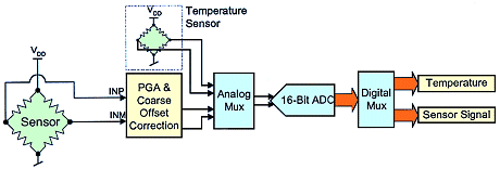 Figure 4. This detail from Figure 3 highlights the architecture for digitizing the temperature and pressure sensor signals. |
A 3-bit plus-sign DAC generates the coarse offset signal, which ranges from nearly 0 to more than ±150 mV.
In addition, the low-level PRT signal must be amplified to make maximum use of the ADC resolution. This is accomplished with a fully differential programmable gain amplifier (PGA), in which four gain settings span the optimum values for today's PRT devices: 46, 61, 77, and 93 V/V. The coarse offset compensated signal is multiplied by one of these gain factors to permit a maximum output voltage swing from the PGA without saturating to either supply rail. This nonsaturating condition applies to all pressure ranges over all temperature ranges.
The differential, 16-bit ![]()
![]() ADC is preceded by an analog multiplexer and followed by a digital multiplexer. Simultan-eous channel selection in these multiplexers routes the coarse offset, amplified differential signal from the PGA to the ADC, and, when the conversion is complete, routes the digital ADC result to the sensor signal register.
ADC is preceded by an analog multiplexer and followed by a digital multiplexer. Simultan-eous channel selection in these multiplexers routes the coarse offset, amplified differential signal from the PGA to the ADC, and, when the conversion is complete, routes the digital ADC result to the sensor signal register.
Coincident with multiplexing the ADC digital output to the temperature register, the differential temperature signal (derived from an integrated temperature-sensitive bridge made from a combination of n-well and polysilicon resistors) is multiplexed to the ADC. The resulting digitized value has a sensitivity of 0.0038 C/LSB and a linearity error of only 1.3 C. The digitized temperature output value corresponding to the ADC's zero output is set to ~25 C.
The DSSP is a reduced instruction set processor (see Figure 5) whose 16 instructions are designed to perform the mathematical operations required in solving the linearization equation above.
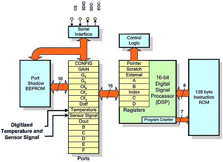 Figure 5. The MAX1460's internal digital sensor signal processor performs the operations required to solve Equation 1. |
In addition, its register-based architecture is limited to 16 registers and 16 ports. The ports are special function 16-bit I/O locations for auto-loading the compensation coefficients from EEPROM, accessing the ADC results, and outputting data to the DAC. The DSP processing engine is 16 bits wide, as are all of the registers.
The digitized temperature and sensor signals arrive in the DSSP's port space as soon as an ADC conversion is completed. Then, the linearization and compensation coefficients of the linearization equation are loaded into predefined ports from the port shadow EEPROM memory. In this way, the DSP can perform 16-bit operations from port data using any of the 16 registers, and transfer the result to a port such as Dout.
Port Dout has a hardwired operation in which it directly drives the 12-bit parallel digital output and the internal 12-bit DAC. When the DSP has completed one iteration of the linearization equation, the result is placed in port Dout. Thus, the equation result is immediately applied to the digital output pins and to the DAC for conversion to an output signal voltage.
Ports B through F are used as general purpose working ports for holding the intermediate calculations necessary in evaluating the linearization equation. The port config contains configuration settings for
|
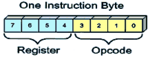
The DSP instructions are stored in ROM that is 1 byte wide (8 bits) and 128 bytes long. Each instruction contains information regarding which register or registers to operate on, and what the operation should be. The instruction byte format is shown in Figure 6, and the instruction set in Table 1.
|
TABLE 1 |
||||
|
The RISC DSP Instruction Set |
||||
|
#
|
Binary
|
Mnemonic
|
Description
|
Cycles
|
|
0
|
0000
|
LDX
|
Load register X from the next 2 words in PS. [PS+1] = high byte, [PS+2] = low byte |
3
|
|
1
|
0001
|
CLX
|
Clear X-reg
|
1
|
|
2
|
0010
|
ANX
|
S-reg = S-reg AND X-reg
|
1
|
|
3
|
0011
|
ORX
|
S-reg = S-reg OR X-reg
|
1
|
|
4
|
0100
|
ADX
|
S-reg ADD X-reg
|
1
|
|
5
|
0101
|
STX
|
X-reg = S-reg
|
1
|
|
6
|
0110
|
SLX
|
Shift Left X-reg, set LSB = 0
|
1
|
|
7
|
0111
|
SRX
|
Shift Right X-reg propagating sign bit
|
1
|
|
8
|
1000
|
INX
|
X-reg = X-reg+1
|
1
|
|
9
|
1001
|
DEX
|
X-reg = X-reg?1
|
1
|
|
10
|
1010
|
NGX
|
X-reg = NOT X-reg
|
1
|
|
11
|
1011
|
BPX
|
Branch Positive or Zero X-reg
|
1
|
|
12
|
1100
|
BNX
|
Branch Not Zero X-reg
|
1
|
|
13
|
1101
|
RDX
|
S-reg = Port-X
|
1
|
|
14
|
1110
|
WRX
|
Port-X = S-reg
|
1
|
|
15
|
1111
|
MLT
|
S-reg | B-reg = A-reg Multiplied By B-reg
|
16
|
The "X" register referred to in each instruction can be any of the 16 registers shown in Table 2.
|
TABLE 2 |
|||||
|
Digital Signal Processor Register |
|||||
|
#
|
Binary
|
Name
|
Description
|
Port In
|
Port Out
|
|
0
|
0000
|
Pointer
|
Instruction pointer
|
DATA
|
OUT
|
|
1
|
0001
|
S
|
Scratch or accumulating register
|
X0 |
|
|
2
|
0010
|
External
|
|
X1 |
|
|
3
|
0011
|
A
|
Multiplicand for the MLT instruction
|
T
|
|
|
4
|
0100
|
B
|
Multiplier for the MLT instruction
|
G0 |
|
|
5
|
0101
|
Index
|
Indexing register
|
G1 |
|
|
6
|
0110
|
C
|
Working register
|
|
|
|
7
|
0111
|
D
|
Working register
|
|
|
|
8-15
|
Not used
|
Reserved for future use
|
Reserved
|
||
Although a complete instruction code for the linearization calculation is not shown, two subroutines are offered: one for the squaring operation (see Listing 1) and one for the multiplication operation (see Listing 2).
|
LISTING 1 |
COMPUTE T^2:
 op-code
 |     line #
       |     mnemonic
             |      comment
                    |
 11    16    CLS    S = 0
 33    17    ORA    S = T
 54    18    STB    B = T
 11    19    CLS    S = 0
 F3    1A    MLT    MULTIPLY, s = T^2/2, B=LSB(T^2/2)
 61    1B    SLS    S = T^2, LSB=0
 53    1C    STA    A = T^2, LSB=0
 11    1D    CLS    S = 0
 34    1E    ORB    S = LSB (T^2/2)
 55    1F    STI    I = LSB (T^2/2)
 B2    20    BPE    IF SIGN BIT OF I=0, JUMP NEXT INTR.
 83    21    INA    A = T^2
|
|
LISTING 2 |
COMPUTE G1 x T/2:
 op-code
 |     line #
       |     mnemonic
             |      comment
                    |
 D2    11    RD2    READ G1 IN S
 54    12    STB    B = G1
 11    13    CLS    S = 0
 F3    14    MLT    MULTIPLY, S = G1.T/2, B=LSB(G1.T/2)
 57    15    STD    D = G1.T/2
|
The result of calculating the linearization equation is output in separate analog and digital formats. To indicate that a new result is available, a 12-bit parallel digital output is provided along with an end of conversion (EOC) signal. The EOC also loads the 12- bit data into a 12-bit ![]()
![]() DAC to generate the analog signal. Necessary filtering of the DAC output is accomplished with an integrated op-amp (see Figure 7).
DAC to generate the analog signal. Necessary filtering of the DAC output is accomplished with an integrated op-amp (see Figure 7).
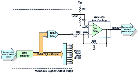 Figure 7. The MAX1460 provides a parallel digital output and, using a DAC, an analog output, filtered here by an external op-amp circuit. |
The entire linearization equation shown in Equation 1 is calculated after two ADC conversions are completed. The first conversion updates the sensor signal port data, and the second updates the temperature port data. The equation calculation is completed in one pass through the 128-byte instruction ROM. At the end of the execution cycle, in which the digital and analog outputs have been updated, the DSP returns to the top of the instruction ROM and awaits completion of two more conversions.
The MAX1460 achieves accuracy >0.5%. To calibrate the sensor assembly (consisting of the MAX1460 and transducer element), measure the assembly output at three temperatures and two sensor excitations, substitute each data item in the characteristic equation, and solve the resulting six equations in six unknowns. For the transducer of Figure 3, nonlinear span and offset errors exceed 8% and 3% respectively. After compensation, its sensor output has span and offset errors less than ±0.05%, as shown in Figure 8.
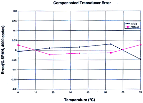 Figure 8. After compensation, the span and offset errors of the sensor shown in Figure 3 are less than ±1.5%. |