
 |
In resistive sensors, pressure changes the resistance by mechanically deforming the sensor, enabling the resistors in a bridge circuit, for example, to detect pressure as a proportional differential voltage across the bridge. Conventional resistive pressure measurement devices include film resistors, strain gauges, metal alloys, and polycrystalline semiconductors.
Monocrystalline silicon pressure sensors have come into wide use in recent years. Though manufactured with semiconductor technology, they also operate on the resistive principle. The resistance change in a monocrystalline semiconductor (a piezoelectric effect) is substantially higher than that in standard strain gauges, whose resistance changes with geometrical changes in the structure. Conductivity in a doped semiconductor is influenced by a change--compression or stretching of the crystal grid--that can be produced by an extremely small mechanical deformation. As a result, the sensitivity of monocrystalline sensors is higher than that of most other types. Specific advantages are:
- High sensitivity, >10 mV/V
- Good linearity at constant temperature
- Ability to track pressure changes without signal hysteresis, up to the destructive limit
Disadvantages are:
- Strong nonlinear dependence of the full-scale signal on temperature (up to 1%/kelvin)
- Large initial offset (up to 100% of full scale or more)
- Strong drift of offset with temperature
Within limits, these disadvantages can be compensated with electronic circuitry.
Manufacturing Piezoresistive Pressure Sensors
For optimal application of these sensors, the user needs to understand their structure, their properties, and how they are made. Monocrystalline silicon in a wafer format provides very high mechanical strength and elastic behavior up to the point of mechanical breakdown, yielding sensors that exhibit only minor response to mechanical aging and hysteresis.
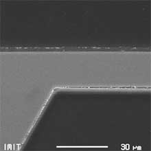 |
| Photo 1. Anisotropic etching achieves extreme precision in fabricating mechanical structures such as the pressure sensor diaphragm shown here in cross section. |
Anisotropically etching the back of a silicon wafer to create round (or square) holes that stop just short of the front surface produces silicon diaphragms with areas up to 7 mm by 7 mm, and thicknesses measuring 5–50 microns, ±1 micron (see Photo 1). The size and thickness of the finished diaphragm depend on the pressure range desired.
Deformation by applied pressure causes high levels of mechanical tension at the edges of the diaphragm. Semiconductor resistors on the front side transduce this tension into resistance changes by means of the piezoresistive effect. Positioning the resistors in this area of highest tension increases sensitivity but at the same time introduces problems. Misregistration of resistors relative to the diaphragm, for example, creates large asymmetries in the resistor bridge that contribute to temperature-dependent errors and nonlinearity in the transfer curve. Even the extreme positioning accuracy of microtechnology reaches its limit in this manufacturing operation.
Because ion implantation replaces only one of every million silicon atoms with a dopant atom, it integrates the resistors monolithically without altering the material's mechanical properties. In contrast to sensors with glued-on resistor stripes, the semiconductor sensor exhibits no mechanical defects from overload or aging.
Via aluminum conductors, the semiconductor resistors are joined together in a bridge configuration and attached to the bond pads for circuit interconnection. The resistors are placed on the diaphragm such that two experience mechanical tension in parallel and the other two are perpendicular to the direction of current flow. Thus, the two pairs exhibit resistance changes opposite to each other. These pairs are located diagonally in the bridge such that applied pressure produces a bridge imbalance (see Photo 2).
Assembly
At one assembly stage, a wafer of ICs is bonded anodically to a wafer of Pyrex glass. (Anodic bonding is a pressure weld in which the two surfaces are pressed together while high current passes through the area of contact.) The bond creates a solid interconnection between the wafers in which mechanical tensions are absent. Because Pyrex and silicon have virtually the same thermal extension coefficients, this connection also avoids thermal tensions. Single chips are then cut from the compound wafer, bonded into a conventional package (often a metal can), and wire-bonded to the package electrical connectors (see Photo 3).
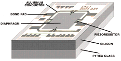 |
| Photo 2. In this silicon pressure sensor, the piezoresistors are joined in a bridge configuration and attached to the bond pads for circuit interconnection. The two pairs are placed diagonally in the bridge such that applied pressure produces a bridge imbalance. |
The method of assembly has a substantial effect on the sensor's characteristic performance. These silicon sensors convert mechanical tension to an electrical signal and cannot distinguish between tensions due to the signal (pressure) and those caused by thermal changes or other effects. The sensor data therefore tend to have a thermal dependency. On the other hand, the fabrication techniques guarantee high precision and large volume at low cost and also allow the integration of compensation resistors and other sensors (temperature types, for instance) on the same piece of silicon.
Pressure sensors are characterized by parameters that depend on the target application. Comparisons are difficult because manufacturers are currently using different terminologies for the same sensor performance parameters. The user should therefore consider the condition of supply voltage and current corresponding to a particular data specification. The most relevant parameters are:
- α. Temperature coefficient of resistance
- Pnom . Nominal pressure range; the pressure range (in bars) for which the sensor complies with given data
- Pmax . Maximum pressure range; the maximum pressure the sensor can withstand without damage
- RB . Overall bridge resistance; the bridge resistance between the supply terminals, which changes with temperature
- αB . Temperature coefficient of bridge resistance; the change in bridge resistance as a function of temperature, in kelvin; useful to the signal-processing circuitry in measuring the sensor temperature
- VOS . Offset; the differential bridge voltage (in millivolts) at constant supply voltage, no pressure applied, and at the reference temperature
- αVOS . Temperature coefficient of offset; the change in offset as a function of the deviation from reference temperature, in millivolts/kelvin; assumes a linear relationship between the temperature and the offset change, which is true only for a limited range
- S. Sensitivity; describes the relationship between the sensor's rate of output change and the applied pressure at the reference temperature; often measured at the full-scale output (FSO)
- αS. Temperature coefficient of sensitivity; the change in sensitivity with temperature
- Linearity. The sensor's voltage/pressure relationship, expressed in terms of offset voltage and sensitivity, is not quite linear; deviations are <1%, but for precision applications they must be considered
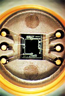 |
| Photo 3. After anodic bonding to a Pyrex glass wafer, the individual chips are cut out of the wafer, bonded into a package such as the metal can shown here, and wire-bonded to the electrical connectors. Because Pyrex and silicon have virtually identical thermal extension coefficients, thermal tensions are eliminated by the bonding step. |
Long-term stability values for the sensor's sensitivity and hysteresis are below 0.1%, and can therefore be disregarded in most applications. For an uncompensated sensor, the relationship for differential output voltage, V DIFF , vs. pressure, P, and temperature, T, is:
V DIFF = V OS + Tα VOS + P(S + Tα S ) (1)
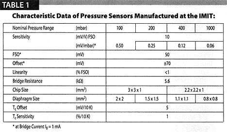
Table 1 gives typical performance data for a series of pressure sensors developed at the Institute for Microelectronics and Information Technology in Germany. Though the diaphram thickness is a constant 15 microns, the devices offer a variation in diaphragm size that provides four different ranges of nominal pressure.
Pressure Sensor Signal Conditioning
As noted earlier, piezoresistive pressure sensors are usable only after corrections have been made for offset and for other effects induced by their sensitivity to temperature variations and by the manufacturing process. Linearity compensation also increases precision, but is not necessary for most applications. For medium-accuracy sensors, a resistor network can compensate for offset, offset drift, and FSO drift (see Figure 1). A low-resistance divider at the bottom of the bridge adjusts for initial offset. The bridge resistors, however, have a positive temperature coefficient that causes the bridge voltage to rise with temperature.
To correct this problem, a resistor, R ts , stabilizes the sensitivity by shunting an increasing amount of excitation current as temperature rises (and with it the bridge voltage, due to increasing bridge resistance). Sensitivity itself has a negative temperature coefficient, so the drift effects work against each other to some extent. In a similar way, another resistor, R tz , works against the change of offset with temperature. These compensation correctives interact with each other, necessitating a calibration scheme that is somewhat cumbersome, of limited accuracy, and virtually impossible to implement as electronic compensation.
A Different Approach to Compensation
 |
| Figure 1. Interaction of the three compensation mechanisms in a conventional resistive compensation circuit (R ts for sensitivity drift, R tz for offset drift, and zero-trim resistors) makes it quite difficult to compensate the overall temperature drift. |
A new family of ICs for conditioning sensor signals (MAX1450, MAX1478, and MAX1457, in order of increasing complexity) takes a different approach to compensation. By decoupling the compensation of offset and sensitivity, these devices allow automatic, high-precision compensation. The recommended combination (a hybrid that includes the sensor chip and a signal-conditioning chip) results in a measurement module that is precise, compact, and interchangeable. It also greatly simplifies the maintenance of field instruments.
The MAX1457, for example, provides electronic compensation of second order linearity errors and higher order temperature effects. Its accuracy is ±0.1% over the operating temperature range. The MAX1478 enables electronic compensation of first-order temperature effects and achieves accuracies better than ±1%. The MAX1450, also accurate to ±1%, targets high-volume applications that require laser trimming. The following discussion explains the basic structure of these devices.
Integrated Compensation Circuitry. In a typical application circuit (see Figure 2), the signal conditioning IC integrates two main functional blocks: a controlled current source for driving the sensor, and a programmable-gain amplifier (PGA). The numerous external resistors and voltage dividers are commonly realized with hybrid technology and adjusted with laser trimming.
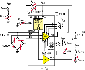 |
| Figure 2. Laser-trimmed resistor dividers in the MAX1450 signal conditioner provide better than 1% compensation full scale over temperature. |
The circuit's initial sensitivity (FSO) is adjusted at the FSOTRIM pin (see Figure 3), and the temperature drift is adjusted by feeding back the sensor's drive voltage (from the BDRIVE pin) to the ISRC pin. Compensation of offset and offset drift is accomplished at the PGA and decoupled from the sensitivity compensation. The PGA itself is implemented in switched-capacitor technology and is virtually free of offset. The key function, however, is the controlled current source, which implements a unique algorithm for compensating the sensitivity drift.
Sensitivity-Drift Compensation. The current mirror in Figure 3 adjusts the bridge current according to the voltage applied at FSOTRIM. Algebraic manipulation allows a derivation of the following relationship between the bridge drive voltage (V BDRIVE ) and the bridge resistance (R B ):
V BDRIVE is proportional to a • V FSOTRIM
• (1/R ISRC + 1/R STC )R B /(1 + aR B /R STC ) (2)
where:
a = mirror factor of the current source
The bridge resistance, R B , and sensitivity, S, are both approximately proportional to temperature:
R B (T) = R B (T = 0)(1 + α B T) (3)
V DIFF (P,V BDRIVE T) = f(P)V BDRIVE
• (1 + α S T) (4)
where:
α B = temperature coefficient of bridge
resistance
α S = temperature coefficient of bridge
sensitivity
V BDRIVE at this point can be considered a free parameter. The expression (T = 0) in Equation (3) represents a selectable reference point such as 0°C.
The following approximations assume that this reference point is inside the sensor's operating range. V DIFF is the sensor's differential voltage between the INP and INM pins, and f(P) gives the sensor's transfer function and linearity, which will be addressed further on. Sensor offset, which is corrected only after the sensitivity is stabilized, is not considered at this point.
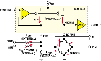 |
| Figure 3. A controlled current source for bridge drive is the core architectural structure for achieving precision better than ±1%. |
V DIFF (P,T) is proportional to P[1 + T
• (α B – α S ) – (α B – α S T 2 )]
• V FSOTRIM (1/R ISRC + 1/R STC )
• R B0 / [1 + a (1 + α B T) (R B0 /R STC )] (5)
Neglecting the higher-order terms that include T 2 , the remaining proportionality is:
V DIFF (P,T) is proportional to
[1 + T(α B – α S )] / [1 + a(1 + α B T)
• (R B0 /R STC )] (6)
 |
| Figure 4. An actual example of uncompensated sensor error demonstrates the difficulty involved in achieving accuracy better than ±0.1% or even ±1% (A). Small errors remain after compensating the signal transducer (B). |
With appropriate adjustment of the RSTC resistor, the sensor's differential voltage can be made independent of temperature changes.
Offset-Drift Compensation. Next, the offset and offset drift must be corrected. Static offset is easily compensated by adding a correction voltage at the PGA input. Offset drift correction is more difficult. As noted above, offset can be approximated as a linear function of temperature and the bridge voltage V BDRIVE (an empirical observation from sensor technology):
V OS (T) = (V BDRIVE ) ( VOS ) (1 + α VOS T) (7)
where:
V OS = offset value at T = 0 relative to the bridge voltage, V BDRIVE
α VOS = temperature coefficient of the offset, which may be positive or negative
V BDRIVE is no longer a free parameter, but instead is determined by the bridge drive circuitry. Sensitivity has been stabilized by choosing the appropriate value for R STC , and a rearrangement of Equation (4) shows that V BDRIVE is now approximately proportional to temperature:
V BDRIVE = V DIFF (P,T) / [f(P)(1 – α S T)] (8a)
V BDRIVE (T) = V DIFF (P) / [f(P)(1 – α S T)] (8b)
Using the Taylor expansion [1/(1 – x)]
= 1 + x + . . ., we obtain:
V BDRIVE (T) . [V DIFF (P) / f(P)]
• (1 + α S T + . . .) (9)
where:
S = sensitivity
S = V DIFF (P) / f(P) (10)
Substituting the V BDRIVE (T) expression from Equation (9) into Equation (7) yields the new offset:
V OS (T) is proportional to S(1 + α S T) VOS
• (1 + α VOS T) (11a)
V OS (T) is proportional to S( VOS )
• [1 + T(α VOS + α S ) + α VOS • α S T 2 ] (11b)
Dropping the small term [(α VOS ) • (α S T 2 )] (again) still leaves a temperature-proportional factor in the expression for offset. Because V BDRIVE is also proportional to temperature, after correcting the initial offset you can compensate the temperature drift of offset by adding (or subtracting, depending on the sign of the offset temperature coefficient) a fraction of V BDRIVE to the PGA output (V OUT ).
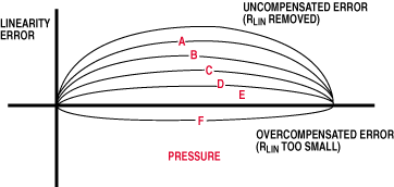 |
| Figure 5. Changing the feedback value (R LIN ) adjusts the linearity error to the user's specification. |
The result is a fully compensated pressure measurement circuit with a two-step approach: The sensor conditioning circuit's input stage (the controlled current source) adjusts to the individual sensor sensitivity as well as the temperature drift of sensitivity, yielding a temperature-independent differential pressure signal plus a bridge-drive voltage that is a linear function of temperature. The second stage eliminates offset errors and the offset temperature drift. This sequence prevents the offset compensation circuitry from adversely affecting the earlier compensation of sensitivity. It requires no repetition, and achieves much better overall precision than does the conventional approach. Figure 4 illustrates the characteristic curves of a sensor before and after compensation.
Transfer-Curve Linearization. Any nonlinearity in the transfer curve of voltage vs. pressure has yet to be taken care of. Such nonlinearity usually resembles a bathtub curve over the measurement range (FSO), and its maximum is typically <1% of the range. MAX145X and 1478 devices allow the user to compensate for this nonlinearity by feeding a fraction of the PGA output (V OUT ) back to the current source control pin (ISRC). This feedback loop has the following transfer function:
V OUT /V DIFF is proportional to P / (1–XP) (12)
where X = feedback ratio determined by resistor R LIN in Figure 2
The resulting compensation is proportional to the amount of feedback (see Figure 5). Because temperature compensation for the MAX1450 is rather coarse, this linearity correction may not be appropriate for all applications. Although the switched capacitor PGA operates in a time-discrete, amplitude-continuous mode, MAX145X and 1478 devices can process pressure changes up to 1 kHz, an unusual capability considering the realizable accuracy of compensation.
Integrating the Compensation Parameters. Circuitry in the MAX1478 replaces numerous external resistive-divider networks by substituting a multiplying D/A converter for each. The resulting IC is a complete signal processor that requires few external components. Its internal D/A converters feature a Σ-Δ architecture, making them very temperature stable. In operation, the necessary compensation coefficients are first written to the internal EEPROM via the serial-data interface. Initial adjustment over temperature, otherwise a time-consuming task, can be implemented on a fully automated, computer-driven measurement and compensation setup.
Compensation circuitry in the MAX1450 and MAX1478 neglects second order temperature effects and incorporates several approximations, while achieving accuracies better than ±1%. For applications that require greater precision, the MAX1457 offers a structure that is similar but provides finer compensation for temperature effects.
The MAX1457 sensor measures the sensor temperature as a function of the sensor's excitation voltage by using an A/D converter. It compensates the first order temperature effects as before, through the voltage-regulation loop. It also stores in an external EEPROM the compensation parameters for sensitivity, sensitivity drift, offset, and offset drift at each of 120 temperature points. This compensation scheme, supported by internal 16-bit D/A converters that require external buffer capacitors for noise reduction, corrects the sensor output for higher order temperature effects. Accuracy is sufficiently high (±0.1%) to justify transfer curve linearization as an additional form of compensation. Because the effect of temperature on this nonlinearity is assumed to be negligible, the chip stores only a single coefficient for linearization (vs. 120 for temperature).
The MAX1457 is programmed and read via an internal serial interface. It includes an uncommitted op amp that may be used to increase the signal gain or control a 420 mA current loop. The resistors for control of the internal current source are external components because using internal resistors would exhibit too much temperature drift.
The above ICs are targeted at applications that require a fast analog signal path to cope with quickly changing inputs, but slower inputs invite a consideration of solutions that feature mostly digital processing. The forthcoming MAX1460 includes a Σ-Δ A/D converter buffered by a PGA, a dedicated RISC processor with sensor-specific ROM code, an EEPROM for coefficient storage, and a D/A converter for analog output. It will enable a new range of applications, including sensor outputs that are strongly nonlinear and wide ranging.