Introduction
In Episode 1 of this series, the concept of critical success factors (CSFs) in their role of technology commercialization was introduced using my annual MEMS Industry Report Card [1]. It also will serve as the basis for addressing several of the CSFs that I believe are also critical to the successful commercialization of printed/flexible/stretchable and functional fabric (P/F/S/&FF) sensors and sensor-based systems. In the next several episodes, several of these CSFs will be addressed using inputs from many the more than 65 interviews that I have conducted as part of a market research study over the past 30 months on this topic. These inputs are from colleagues who are highly experienced practitioners in these various area and several of whom will join me with their presentations at the upcoming all-day June 26 preconference on this topic, Commercialization of Printed/Flexible/Stretchable and Functional Fabric Sensors and Sensor-Based Systems for IoT and Wearables” at Sensors Expo 2018 in San Jose California, which I have organized and will chair.
In this episode, we will first address the compelling factors for the adoption of P/F/S&FF technologies and then address what I consider to be one of the most significant CSFs, design for manufacturing and test where packaging, device design driven by software tools and reliability will be addressed. Noteworthy, is that design for manufacturing and test is one of the 14 CSFs addressed in my annual MEMS Industry Commercialization Report Card Market Study.
Compelling Factors for Adoption
In our article, Trillion Sensors Initiative [2], Dr. Janusz Bryzek and I stated that reducing the average cost of a sensor is a necessary requirement for achieving the trillion-sensor goal, i.e., for the worldwide annual volume of sensors shipped to reach the trillion-unit level. The opportunity to collaborate with Janusz on his Trillion Sensor Initiative was a catalyst to my involvement in P/F/S and FF technologies and the undertaking of my major market study where I have interviewed to date over 65 industry leaders in these technologies. The success of the Trillion Sensors Initiative will be accomplished to a great deal by the widespread adoption of ultra-low-cost sensors, many being fabricated from paper, plastic or threads/fabrics. Sensors using low-cost substrates are the key to this.
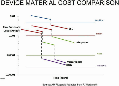
It has been noted by several industry pundits that the cost of paper- and plastic-based sensor materials are approximately two orders of magnitude less expensive on a square area perspective than those made from silicon, the material of choice for today’s popular MEMS devices (Fig. 1). This alone is a compelling factor for the accelerated adoption of these technologies. Another is their physical shape, ability to be made in large arrays, low- profile and especially their ability to conform and be in direct contact with complex three-dimensional structures, for example, the human body, making them ideally suited for wearable applications.

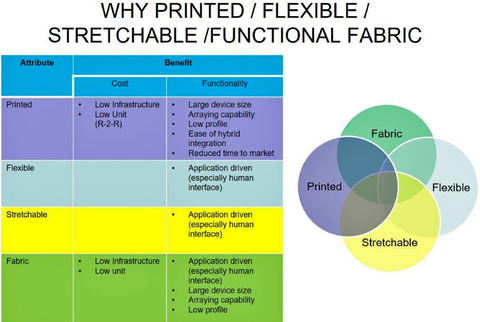
For any new technology to be successful, there needs to be a market and applications pull and not a technology push as discussed in my previous article on “Sensors and MEMS Marketing: Oxymoron or Opportunity” which recently appeared in this publication [3]. Organizations must listen to the voice of the customer (VOC) to best plan products and select technologies that will meet new application opportunity requirements. Fig.2 shows the cost and functionality benefits of P/F/S and FF sensors and electronics. Enhanced functionality and cost are major customer/market benefits.

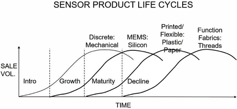
In addition, I believe that the advent of PFS and following that… FF sensors and sensor-based systems will be the next two waves of sensor innovation/product life cycle preceded by MEMS/Silicon and discrete/electromechanical platforms. Fig. 3. The four phases of the sensor product life cycle process are:
• Introduction
• Growth
• Maturity
• Decline
MEMS, which typically use a Silicon platform, became ubiquitous with their widespread introduction into mobile phones, achieved their level of maturity in the mid-late 2000’s. They are now considered commoditized. P/F/S and FF are in their introduction phases. I believe that now is the time for the development of these technologies to be added to the “toolkits” of product designers.

Critical Success Factors
As stated previously, the MEMS Industry Commercialization Report Card topics a.k.a. CSFs were the basis to select the CSFs relevant to P/F/S&FF technologies. Furthermore, I have conducted market research interviews with many industry pundits to obtain their observations and opinions on these CSFs. The following are excerpts from these interviews relevant to the topic design for manufacturing and test.
Packaging & Interconnects
A major element in successful commercialization of these technologies is the development of packaging/interconnects strategies. There is much to be learned from the integrated circuit (IC) as well as the MEMS industry on this topic [4].
The future success of P/F/S &FF electronics (and their associated sensors) resides in the ability of suppliers to judiciously select the required functionalities of the individual circuit functions and determine the optimum format i.e. Silicon, plastic or paper for their realization in specific applications and their integration into an optimum solution for those applications. Packaging and interconnect considerations for P/F/S&FF sensors and sensor-based systems include the following:
• thorough assessment of monolithic versus heterogeneous versus hybrid integration strategies;
• adopting a systems solutions approach [5] where the sensor is an integral and important part of an assemblage of various electronic functionalities and packaging/interconnects which provide an entire solution to the client’s application
• connectivity of individual devices to each other and to the substrate;
• packaging/encapsulating of the total solution
• creation of models and software tools for the design/layout and reliability determination of these technologies; and
• determination of the manufacturing/integration/assembly method to minimize cost and maximize functionality and reliability.
Dr. Leland (Chip) Spangler, founder and CEO of Aspen Microsystems—a provider of MEMS and microelectronics product design and consultancy services and a 30 plus-year veteran of the MEMS industry said, “Sensors face many of the same issues regardless of the technologies that are used to make them. The fidelity of a sensor’s signal and its reliability can be impacted by stress, temperature and electromagnetic fields, so a practical sensor must be impervious to these stresses while still providing the sensitivity to the desired factor to be sensed.
“MEMS and silicon-based sensors benefit from the huge infrastructure and deep scientific understanding of materials and processes from the IC industry. These devices often have an explicit package that can be optimized specifically for the application. P/F/S and FF sensors represent a fundamentally new sensing paradigm and thus cannot leverage an existing infrastructure of knowledge. These types of devices will require new materials, manufacturing methods and scientific knowledge, which will require a great deal of investment. Since P/F/S and FF sensors have no explicit package, the materials and structures that perform the sensing function must also perform the packaging function by providing robustness over long periods of time while being used by consumers in wide ranging conditions, all without degrading the desired sensor signal. This will be a huge challenge to overcome.”
Reliability
For P/F/S and FF-based sensors and electronics to find their way into current and future products, reliability analysis is critical. Allyson Hartzell is managing engineer at Veryst Engineering—an engineering consultancy and services provider for product manufacturing, co-author of a recent book on MEMS Reliability [6] and a 20 plus -year veteran of the MEMS industry. She said: “Knowledge of known failure mechanisms, material properties and assembly methods can result in reducing cycle times through designing for manufacturing, yield and reliability. With new technologies, there will always be new failure mechanisms that are unknown, but if a company in the early stages can develop a product that doesn’t succumb to already known failure mechanisms, the product has a higher probability of success.”
She continued, “For instance, new developments in interconnect technology for P/F/S and FF sensors is of high priority. The same can be said of multi-chip packaging, which allows sensors and microprocessors to be packaged in a very tiny form factor. Coupling the sensor packaging and, for instance, a flexible interconnect, you will still have the need for low-contact resistance over time with a low-loss interconnect that provides the proper impedance and conductivity without early failure.”
Software Tools and Design
Finally, designers and developers of these technologies require the software tools to design and develop the devices/systems. Once again, lessons learned from the IC and MEMS industries play a vital role in this learning process. Dr. Mary Ann Maher, the founder and CEO of SoftMEMS, a provider of these software tools and another 20 plus-year veteran of the MEMS industry, shared her views, “The MEMS market has matured to the point that there is now a strong supplier ecosystem in-place to support the required design of manufacturing and test activities. This ecosystem is still developing for P/F/S and FF sensors. The flexibility of these sensors adds complexity with regards to their modelling, testing, reliability and performance specification.”
She concluded, “Some similarities between the two technologies are that there are a variety of manufacturing methods and materials used to create devices and products and few standard device structures and models, i.e. intellectual property (IP) as in the IC industry. One of the current promising technology approaches is the combination of mature MEMS devices and flexible substrates.”
Summary & Conclusions
In Episode 2, the motivations for the adoption of P/F/S&FF sensors and sensor-based systems have been presented…and which, when distilled, come down to reduced cost per device and higher functionality…especially in their shape conformity which makes them ideal for wearable applications. It is critical that organizations listen to the voice of the customer (VOC) in the development of new technologies for new applications and not just create technologies for technologies-sake. Adopting a “build it and they will come” strategy will not work in product development, only in Hollywood in movies like Field of Dreams.
Additionally, the first of many critical success factors (CSFs), design for manufacturing and test was specifically addressed using inputs from several industry pundits in their specific areas of expertise including packaging, reliability and software tools for design. I believe that there is a great deal of knowledge that can be taken from our experience with the commercialization of MEMS.
Again, MEMS greatly benefitted from the successful commercialization of integrated circuits. And to use one of my most favorite quotes from George Santayana, “those who forget the past are condemned to relive it” [7]. Bottom line, we need to learn from our successes as well as from our failures. In our next episode, several other CSFs including manufacturing infrastructure and discussions regarding batch versus continuous, i.e., roll-to-roll printing processes will be addressed.
Learn More
I have organized and will chair an all-day Preconference Symposia on the “Commercialization of Printed/Flexible/Stretchable and Functional Fabric Sensors and Sensor-Based Systems for IoT and Wearables” at Sensors Expo 2018 on June 26, 2018 at the San Jose California Convention Center where I will be joined by 14 renowned experts on this topic. For more information including agenda, abstracts’, presenter bios, and registration information, visit Sensors Expo 2018. Use the registration code Rgrace100 to receive a registration discount.
I am also organizing and will chair a technical session on the same topic at the MANCEF Commercialization of Micro, Nano and Emerging Technologies to be held in Montreux, Switzerland; September 24-26, 2018. For registration information, visit MANCEF. There are still several presentations opportunities in my session and at the Conference. For more information, contact me via email at [email protected].
REFERENCES
[1] R. Grace; Barriers to the Commercialization of MEMS: The 2014 MEMS Industry Commercialization Report Card, Commercial Micromanufacturing International; Vol. 8, No. 5
[2] J. Bryzek, R. Grace; Trillion Sensor Initiative; Commercial Micromanufacturing International; Vol. 7, No. 2
[3] R. Grace, Sensors/MEMS Marketing: Oxymoron or Opportunity, Episode 1, Sensors Online, September 2017
[4] M. Apainus, R. Grace, M. Maher, J. Mitchell; MEMS-Based Systems Solutions: Packaging; Commercial Micromanufacturing International; Vol. 5, No. 6
[5] R. Grace; Think Outside the Chip: MEMS-Based Systems Solutions; MEMS Technical Review; Vol. 1, No.7
[6] A. Hartzell, M. DaSilva, H. Shea; MEMS Reliability; Springer Publishing; Berlin, Germany;2011; 291 pp.
[7] G. Santayana, Life of Reason, 1905
About the author
Roger H. Grace is president of Roger Grace Associates (RGA), a Naples Florida-based marketing consulting firm specializing in high technology, which he founded in 1982. His background includes over 40 years in analog circuit design engineering, manufacturing engineering, application engineering, project management, product marketing, and technology consulting. He can be reached at 239-596-8738, [email protected].