
Noncontact capacitive sensors measure the changes in an electrical property called capacitance. Capacitance describes how two conductive objects with a space between them respond to a voltage difference applied to them. A voltage applied to the conductors creates an electric field between them, causing positive and negative charges to collect on each object (Figure 1). If the polarity of the voltage is reversed, the charges will also reverse.
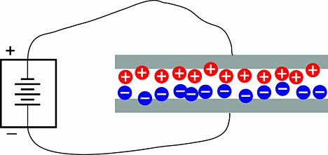 Figure 1. Applying a voltage to conductive objects causes positive and negative charges to collect on each object. This creates an electric field in the space between the objects |
Capacitive sensors use an alternating voltage that causes the charges to continually reverse their positions. The movement of the charges creates an alternating electric current that is detected by the sensor (Figure 2). The amount of current flow is determined by the capacitance, and the capacitance is determined by the surface area and proximity of the conductive objects. Larger and closer objects cause greater current than smaller and more distant objects. Capacitance is also affected by the type of nonconductive material in the gap between the objects. Technically speaking, the capacitance is directly proportional to the surface area of the objects and the dielectric constant of the material between them, and inversely proportional to the distance between them as shown in Equation 1:
| (1) |
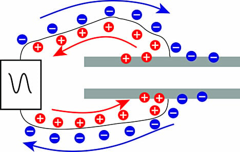 Figure 2. Applying an alternating voltage causes the charges to move back and forth between the objects, creating an alternating current that is detected by the sensor |
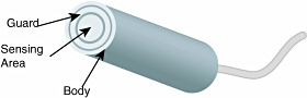 Figure 3. Capacitive sensor probe components |
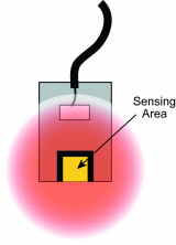 Figure 4. Cutaway view showing an unguarded sensing area electric field |
Focusing the Electric Field
When a voltage is applied to a conductor, the electric field emanates from every surface. In a capacitive sensor, the sensing voltage is applied to the sensing area of the probe (Figures 3 and 4). For accurate measurements, the electric field from the sensing area needs to be contained within the space between the probe and the target. If the electric field is allowed to spread to other items—or other areas on
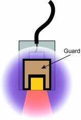 Figure 5. Cutaway showing the guard field shaping the sensing area electric field |
Definitions
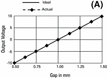
Sensitivity indicates how much the output voltage changes as a result of a change in the gap between the target and the probe. A common sensitivity is 1 V/0.1 mm. This means that for every 0.1 mm of change in the gap, the output voltage will change 1 V. When the output voltage is plotted against the gap size, the slope of the line is the sensitivity (Figure 6A).
A system's sensitivity is set during calibration. When sensitivity deviates from the ideal value this is called sensitivity error, gain error, or scaling error. Since sensitivity is the slope of a line, sensitivity error is usually presented as a percentage of slope, a comparison of the ideal slope with the actual slope (Figure 6B).
 |  |
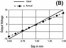 | 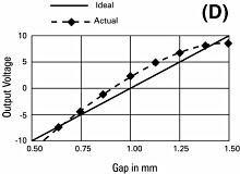 |
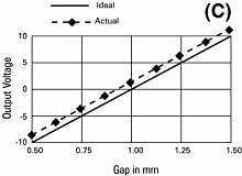
| Figure 6. Illustrating some of the basic definitions. Sensitivity (A) is the slope of the line; in this case 1 V/0.05 mm. Sensitivity error (B) occurs when the slope of the actual measurements deviates from the ideal slope. In offset error (C), a constant value is added to all measurements. Linearity error (D) occurs when measurement data are not on a straight line (Click an image for a larger version) | |
Offset error (Figure 6C) occurs when a constant value is added to the output voltage of the system. Capacitive gauging systems are usually "zeroed" during setup, eliminating any offset deviations from the original calibration. However, should the offset error change after the system is zeroed, error will be introduced into the measurement. Temperature change is the primary factor in offset error.
Sensitivity can vary slightly between any two points of data. The accumulated effect of this variation is called linearity error (Figure 6D). The linearity specification is the measurement of how far the output varies from a straight line.
To calculate the linearity error, calibration data are compared to the straight line that would best fit the points. This straight reference line is calculated from the calibration data using least squares fitting. The amount of error at the point on the calibration line furthest away from this ideal line is the linearity error. Linearity error is usually expressed in terms of percent of full scale (%/F.S.). If the error at the worst point is 0.001 mm and the full scale range of the calibration is 1 mm, the linearity error will be 0.1%.
Note that linearity error does not account for errors in sensitivity. It is only a measure of the straightness of the line rather than the slope of the line. A system with gross sensitivity errors can still be very linear.
Error band accounts for the combination of linearity and sensitivity errors. It is the measurement of the worst-case absolute error in the calibrated range. The error band is calculated by comparing the output voltages at specific gaps to their expected value. The worst-case error from this comparison is listed as the system's error band. In Figure 7, the worst-case error occurs for a 0.50 mm gap and the error band (in bold) is –0.010.
Figure 7. Error values
| Gap (mm) | Expected Value (VDC) | Actual Value VDC) | Error (mm) |
| 0.50 | –10.000 | –9.800 | –0.010 |
| 0.75 | –5.000 | –4.900 | –0.005 |
| 1.00 | 0.000 | 0.000 | 0.000 |
| 1.25 | 5.000 | 5.000 | 0.000 |
| 1.50 | 10.000 | 10.100 | 0.005 |
Bandwidth is defined as the frequency at which the output falls to –3 dB, a frequency that is also called the cutoff frequency. A –3 dB drop in the signal level is an approximately 30% decrease. With a 15 kHz bandwidth, a change of ±1 V at low frequency will only produce a ±0.7 V change at 15 kHz. Wide-bandwidth sensors can sense high-frequency motion and provide fast-responding outputs to maximize the phase margin when used in servo-control feedback systems; however, lower-bandwidth sensors will have reduced output noise which means higher resolution. Some sensors provide selectable bandwidth to maximize either resolution or response time.
Resolution is defined as the smallest reliable measurement that a system can make. The resolution of a measurement system must be better than the final accuracy the measurement requires. If you need to know a measurement within 0.02 µm, then the resolution of the measurement system must be better than 0.02 µm.
The primary determining factor of resolution is electrical noise. Electrical noise appears in the output voltage causing small instantaneous errors in the output. Even when the probe/target gap is perfectly constant, the output voltage of the driver has some small but measurable amount of noise that would seem to indicate that the gap is changing. This noise is inherent in electronic components and can be minimized, but never eliminated.
If a driver has an output noise of 0.002 V with a sensitivity of 10 V/1 mm, then it has an output noise of 0.000,2 mm (0.2 µm). This means that at any instant in time, the output could have an error of 0.2 µm.
The amount of noise in the output is directly related to bandwidth. Generally speaking, noise is distributed over a wide range of frequencies. If the higher frequencies are filtered before the output, the result is less noise and better resolution (Figures 8, 9). When examining resolution specifications, it is critical to know at what bandwidth the specifications apply.
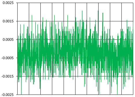 Figure 8. Noise from a 15 kHz sensor |
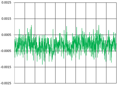 Figure 9. Noise from a 100 Hz sensor |
Next month, in the second part of this article, we'll apply these basic principles and discuss how to optimize the performance of capacitive sensors when dealing with targets of various sizes, shapes, and materials.
Editor's note: The figures in the articles are numbered consecutively.