

The Challenge
Portability of battery-powered devices is growing in all fields. With smartphones now ubiquitous, individuals across the globe have rising expectations for additional mobility.
Because of the low cost and low power of the smartphone chip sets, battery-powered devices are at the heart of virtually all portable devices. More than ever, devices such as application processors, wireless modems, cameras, and displays are adopted for numerous products. In particular, a wide range of portable product applications employ cameras and displays. However, many design challenges appear as these devices move further away from the smartphone-specific architecture.
One issue is the camera or display interface connections to non-application processor devices. Another issue is that unique peripherals, such as thermal image sensors or bar code scanners, are not found on a smartphone. These issues are problematic for architects who want to build portable products and leverage some of the smartphone chip sets. The question is, how can these design challenges be addressed?
Know Thy Architecture
To understand where the design challenge starts, one must be familiar with the smart phone and tablet key components (figure 1). The high volume of this platform can be leveraged by other applications. But why is the smartphone chip set so widely used in other products? The smartphone chip set is the logical starting point because its architecture has many features required at the lowest power and at aggressive cost points needed for the vast majority of portable products in medical, industrial, and other markets.
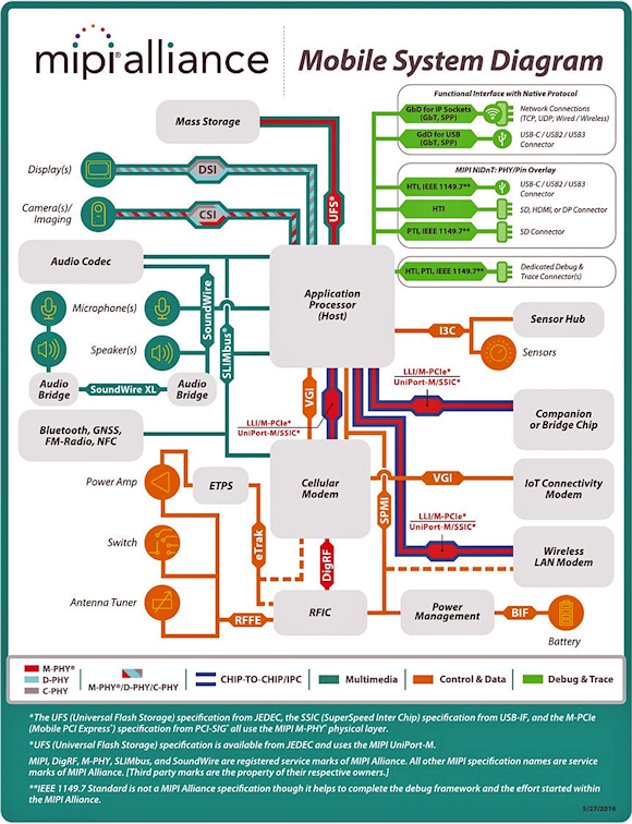
Fig. 1: MIPI Alliance Mobile System Diagram
As you can see, the core is the application processor—it is low power, highly capable, and supports many common peripheral interfaces. And the camera and displays found in many smartphones are even more widely used than the processor in embedded designs. The image sensors specifically are very compact, low power, and high quality.
Next page
The Smartphone Camera
The smartphone image sensor is often the logical product choice for portables. Let us look at a few product examples and their specific challenges.
First, let's consider the thermal image camera design for a hand-held industrial application. As stated previously, a good starting point may be the application processor—it can drive a display, connect to wireless network modems, and interface to on-board storage for saving images or video. However, an application processor cannot directly connect to the majority of thermal sensors.
The smartphone image senor has a second generation Camera Serial Interface (MIPI CSI-2) that exists on an application processor, but a thermal sensor most commonly uses a CMOS parallel or LVDS interface. A small, low-power FPGA could be designed to bridge CMOS parallel to CSI-2, but it would have to generate so little heat that the thermal sensor is not disrupted. Also, the CSI-2 interface of the application processor is not designed to interface to pixels that read temperatures as the thermal sensor does. Instead, the application processor expects color pixel data. This mismatch means that another device has to implement the image processing for the thermal sensor.
A low-power FPGA would be a good choice if it consumes little power, generates very little heat, and can interface to the application's processor with an adequate bus speed. The most common processor interface with good throughput is the PCIe bus.
Selecting a low-power FPGA with PCIe that does not generate heat to disrupt the thermal sensor is paramount. A good choice is the IGLOO2 flash-based FPGA, which has much lower power consumption than SRAM-based FPGAs, do not generate much heat, and have built-in PCIe Gen2 cores in hard logic. In addition, this single chip FPGA is offered in a package as small as 11 mm x 11 mm.
In this application, the IGLOO2 FPGA interfaces to the thermal sensor and performs the necessary processing (figure 2). It converts the temperature data to corresponding colors from a selected palette that can be stored in the on-chip flash or embedded memory blocks. Each line is processed and then formatted to be sent out through the PCIe to the application processor. After the image is received, the processor can then drive it out to the display, save it to local storage, or send it out through a wireless modem. The combination of the FPGA and other smartphone chips can build a compelling thermal camera for industrial, medical, military, and other markets.
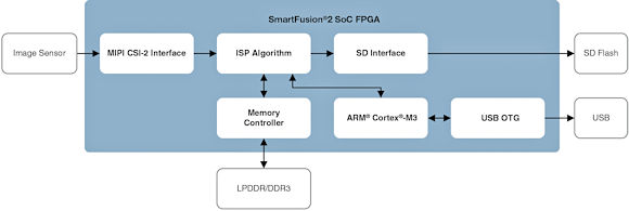
Fig. 2: Block Diagram of a Thermal Image Camera
Next page
Time-Lapse Camera
Another design example we can explore is a time-lapse camera, which captures slow changing content anywhere from once per second to once an hour or even once per day. It is a portable battery-powered device that must capture and store images in between powering-up and shutting-off quickly to preserve power. It can capture flowers growing, sunsets, and buildings being constructed. Because of the content they are capturing, time lapse cameras have to operate on batteries for periods up to several months.
In this design, the logical choice is an image sensor originally designed for a smartphone. On the other hand, the application sensor is not a great choice. Although application processors are low power when off, they consume lots of power when on. They also take indefinite time before going back to a very low-power mode, which drains the battery.
A better choice is a low-power FPGA that powers up instantly, has DSP blocks to implement the image processing, and can interface to CSI-2 for the image sensor interface. In addition, it would be more power efficient to use a low-end microcontroller to handle storing the images to external flash, as well as managing the USB interface when downloading to a PC. Therefore, the flash-based SmartFusion2 SoC FPGA is an excellent choice. It is low power, instant on, and incorporates a Cortex ARM M3 with a microcontroller subsystem that includes a USB OTG core. The SmartFusion2 also has built-in DSP blocks, adequate logic, embedded memory blocks and can interface directly to CSI-2 for the image sensor (figure 3).
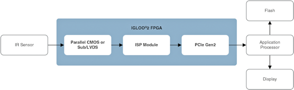
Fig. 3: Block Diagram of a Time Lapse Camera
In this design, the FPGA interfaces to the image sensor and the image processing is done in the DSP blocks embedded memory as well as the FPGA fabric. The SmartFusion2 is on as soon as the camera powers up. Frames are captured and processed by the FPGA and stored to on-board flash. Once all tasks are complete, the camera and FPGA quickly power down.
Although most of the functions in this design could be done by a SRAM FPGA, the power consumption and initialization time required to start up—not to mention the spike of in-rush current that must be absorbed by the battery—makes SRAM technology less than ideal. The flash-based SmartFusion2 has very low static power and total power, which is ideal for this battery-powered design. And the icing on the cake; this device also incorporates a built-in Cortex ARM M3 and USB OTG controller that enables the stored images to be transferred to a PC for future editing or viewing.
Going Forward
The trend for portable products will likely continue to grow. The challenges that designers face when using only some of the components from the smartphone architecture can be addressed.
One solution is to leverage low power, flash-based FPGAs and flash-based SoC FPGAs. With these options available to system architects, numerous device combinations are possible to create an optimal portable product.
About the Author
Ted Marena is the director of FPGA/SOC marketing at Microsemi. He has over 20 years' experience in FPGAs. Previously Marena has held roles in design engineering, technical sales/support, business development, product & strategic marketing. He was awarded Innovator of the Year in February 2014 when he worked for Lattice Semiconductor. Ted holds a Bachelor of Science in electrical engineering Magna Cum Laude from the University of Connecticut and a MBA from Bentley College's Elkin B. McCallum Graduate School of Business.
Related Stories
The Growing World of the Image Sensors Market
Image Sensors for a Smart Environment
The Future of Image Sensors is Chip Stacking