

Tempe, AZ — A team of ASU engineers, including Sefaattin Tongay, an assistant professor of materials science engineering at the Fulton Schools, is reporting for the first time an extraordinary and tunable interlayer electron-phonon interaction in WSe2/hBN heterostructure. The discovery makes a significant step forward in fundamental understanding of van der Waals heterostructures — two-dimensional atomic crystals — and enables new pathways to engineer electrons and phonons for novel device applications.
An article about the breakthrough, “Interlayer electron–phonon coupling inWSe2/hBN heterostructure,” was published in Nature Physics Magazine.
In addition to the ASU team, researchers at the University of California, Berkeley and the Japan National Institute for Materials Science, Advanced Materials Laboratory participated in the project. Bin Chen and Xi Fan, both ASU materials science graduate research associates, were responsible manufacturing and synthesis of extremely high quality, defect-free 2D material systems that are necessary for the success of this project.
“We are looking at atomically thin materials in this work,” said Sefaattin. “These materials find new and exciting applications especially when they are placed onto each other. In this work, we are trying to shed further light on how these unique material systems behave when they are stacked onto each other on demand and when they interact rather strongly. We find that atomic vibrations and electrons interact in a way that new properties emerge from these interactions.”
Potential applications of 2D heterostructures include field effect/tunneling transistors, biosensors, light emitting diodes, light detectors, photovoltaic and energy storage devices.
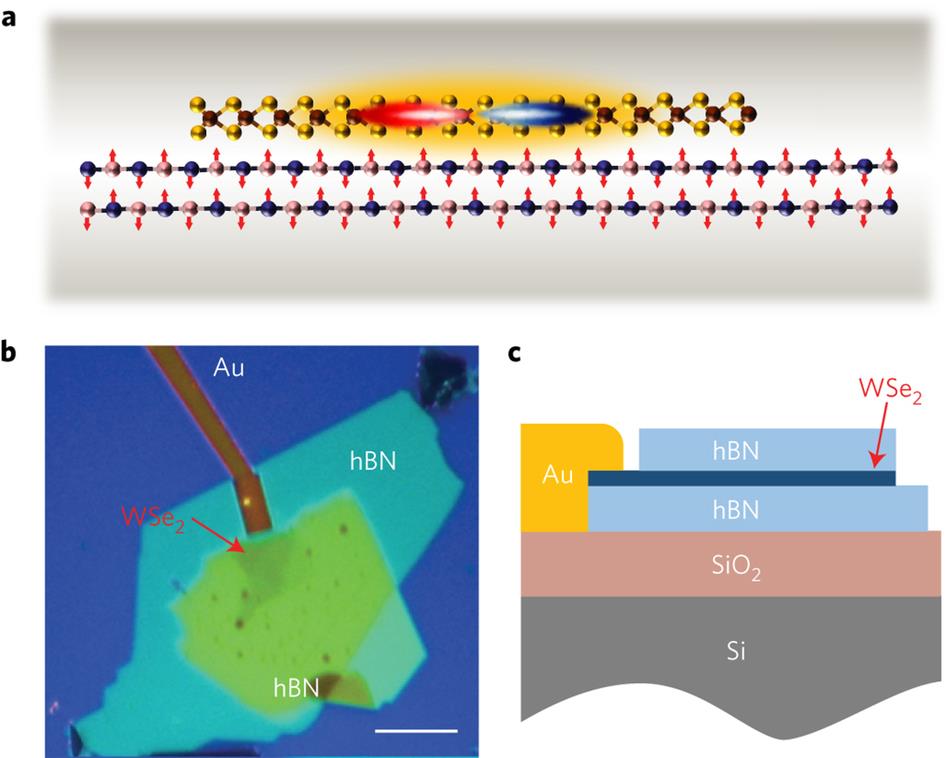
(a) Illustration of interlayer electron–phonon coupling. Red arrows in hBN (bottom) and red/blue clouds in WSe2 (top) show schematically the phonon vibration in hBN and the electron/hole states in WSe2, respectively. Such interlayer electron–phonon interactions can lead to novel electronic and optical properties in the van der Waals heterostructure. (b) Optical microscope image of WSe2 encapsulated in hBN layers. The scale bar corresponds to 5 μm. (c) Illustration of the gate-tunable device. A contact electrode (Au/Ti) is fabricated on the exposed part of WSe2 outside the top hBN layer to allow for electrostatic gating.