
The demand for sensitive, low-power, low-cost gas sensors that respond quickly to appropriate stimuli is growing. Macro scale components and conventional manufacturing techniques cannot provide sensors that deliver the detection levels and low-power operation increasingly required by today's applications. And many of these sensors are prone to false alarms. However, manipulating sensing events at the molecular level avoids most problems associated with the more traditional sensor technologies.
Nanotechnology and Sensing
Nanotechnology offers a unique advantage to the sensor industry by manipulating materials at the molecular level, where sensing events occur. Potentially, the technology offers devices with greater sensitivity, selectivity, and reliability than conventional semiconductor, electrochemical, and optical sensors.
Attaining these advantages is not without challenges. Sensor manufacturers encounter difficulties in manufacturing nanostructures, controlling their behavior from the micro to the macro scale, reading reliable responses, and compensating for small signal drift. In short, the nanosensors business is extremely attractive, but it is fragmented and requires a flexible and robust commercialization strategy.
Multipurpose Platforms
To overcome these obstacles, Applied Nanotech Inc. (ANI), a developer of nano gas sensors, is pursuing a multipurpose-platform approach. Conventional sensor manufacturers respond to a need and develop a technology adequate for a specific sensing event. This approach is one of the main reasons for the fragmentation the industry is encountering. By applying a multipurpose-platform approach, ANI customizes its basic sensor platform to produce a variety of gas sensors (i.e., each can detect different gases). The company has developed four platforms (Figure 1) that use the major gas sensor technologies: gated metal-oxide semiconductor (GMOS) sensors, metal nanoparticle sensors, enzyme-coated carbon nanotubes, and photoacoustic sensors. Each platform is based on existing core components and an understanding of the particular sensing mechanism at the molecular and nano levels. This enables the multipurpose platforms to respond to a variety of sensing events and offer the robustness and flexibility required for the commercialization of sensor products.
 Figure 1. ANI sensor platforms |
Gated Metal-Oxide Sensors. ANI's GMOS-based platform has replaced the thermal requirement of metal oxide semiconductor (MOS) sensors with an electronic gate bias (Figure 2). This platform offers enhanced environmental stability, low-power operation, and high sensitivity. Traditional MOS sensors operate with surface temperatures of 250°C–600°C, requiring the use of a heated substrate, which is often fragile. The sensors require high power (0.5–2 W) to operate the onchip heaters, limiting the robustness and battery life of the sensors in portable applications. The GMOS platform solves these problems, and because of its low power consumption (nW/sensor element) is well suited for wireless applications.
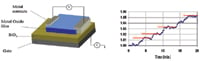 Figure 2. Gated metal-oxide semiconductor sensor architecture (A) and CO sensor response (B) |
The immediate application for this platform is CO sensing. ANI has developed a GMOS CO sensor that requires no heating and has the potential for high selectivity, sensitivity, and specificity. The sensor operates on low power and has a demonstrated CO detection limit of 2 ppm (Figure 2). But the same device has the potential to reach much lower detection levels. The sensor also operates down to –60°C without a heater, a capability that is not available with MOS gas sensors. The GMOS-based platform has industrial and commercial applications in monitoring home safety, mines, vehicles, aircraft, and office and industrial buildings. The company is developing the CO sensor for military applications and intends to extend the platform to detect multiple gases in military and commercial applications.
Metal Nanoparticle Sensors (MNPS). ANI's first product based on the MNPS platform is a palladium nanoparticle-based hydrogen sensor. Nanoparticles of palladium provide a high surface-to-bulk ratio compared with macro scale palladium thin films used for hydrogen sensing. Nanoparticles have a higher percentage of active surface atoms, which detect molecular events more effectively and maximize sensor signal in comparison with thin-film devices. The effective volume of palladium nanoparticles increases in the presence of hydrogen, causing electrical shorts within a random network (Figure 3), resulting in a change of electrical conductivity.
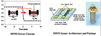 Figure 3. Metal nanoparticle sensor (MNPS) concept (A), architecture (B) , and package (C) |
Using palladium nanoparticles as the active sensing material has solved the problems associated with thin-film palladium resistors. A network of nanoparticles is placed on the sensor element by metal electrodeposition. The electrical conductivity of the nanoparticle networks increases with exposure to hydrogen due to the bridging of the electrical pathways between individual nanoparticles. The sensor can be tuned for different concentration ranges by precisely controlling the size distribution and distance between one nanoparticle and another. The sensor contains a variety of nanoparticle networks that provides a broad dynamic sensitivity range for hydrogen (10–40,000 ppm). The sensor has a logarithmic response to hydrogen and consumes low power (nW). The low power consumption makes the sensor attractive for wireless applications. The hydrogen sensor chip is 4 × 4 mm2 and fits on a TO-5 package. The sensor terminals are wire-bonded to the package leader leads.
ANI has engineered the sensor for operation in harsh environments by using a thermoelectric cooler (TEC) for thermal stability. The TEC element maintains a constant sensor temperature, which enables stable sensor operation and dramatically simplifies its calibration, eliminating the need to compensate temperature effects on sensor response. The company has developed complete drive electronics and calibration protocols for sensor operation. Because of its broad dynamic range and operational stability, the sensor can detect hydrogen in both gas and liquid phases. This hydrogen sensor is the only nanotechnology-enabled sensor used for continuous monitoring of hydrogen levels in transformer insulating oil. ANI is pursuing applications in fuel cells, hydrogen-powered vehicles, and IC engines for hydrogen gas detection.
Enzyme-Coated Carbon Nanotubes (ECNT). ANI's ECNT-based electrochemical biosensor platform is designed to meet the demand for medical, environmental, and chemical analysis. Carbon nanotubes have a 3D network that offers excellent stability, promotes enhanced enzyme loading, and provides increased analyte exposure. Nanotubes are coated uniformly with an enzyme specific to the desired analyte (Figure 4) for excellent sensitivity and selectivity. The ECNT-based electronic tongue can analyze a large number of analytes from a single drop of blood, urine, or saliva for metabolic analysis. In addition to metabolic sensing, the ECNT electronic nose can perform similar functions for toxic gas detection and chemical warfare sensing.
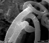 Figure 4. Scanning electron micrograph of enzyme-coated carbon nanotubes |
Photo Acoustic Sensors (PAS). ANI is also developing a simplified PAS platform capable of identifying trace amounts of most gases and vapors. It is also miniaturizing and improving the sensitivity of the PAS platform down to ppb levels.
Rapid Product Development
ANI is addressing critical problems in the gas sensor industry using nanotechnology and a unique platform approach. This approach enables rapid product development because the R&D efforts applied to one sensor in a platform can be readily applied to a suite of sensors. The electronic drivers, sensor packaging, software, and noise compensation are developed at the platform level and fine-tuned at the sensor level. This results in reduced costs, improved sensor efficiency, and enhanced performance using nano-enabled sensors.
Zvi Yaniv, PhD, and Prabhu Soundarrajan, MS, can be reached at Applied Nanotech Inc., Austin, TX; 512-339-5020, x-103, [email protected], www.nanoproprietary.com.