
The piezoresistive property of silicon is well known, and its value as a strain gauge has been recognized by load cell manufacturers for more than 50 years [1]. In fact, Wheatstone bridges, consisting of silicon piezoresistors on a silicon microdiaphragm, enabled the first microelectromechanical systems (MEMS) pressure sensing devices in the 1970s, and endures as a dominant architecture for many MEMS applications. Despite its high gauge factor, typically 30–120 [2], the silicon strain gauge has been relegated to a small niche in today's total strain gauge market.
Metal foil gauges continue to dominate, although their gauge factors are about two orders of magnitude lower, typically 2–5. There are several reasons for this.
Because the metal is sputtered directly onto polyimide or other flexible backing, foil gauges are easy to handle and use. Commercially available silicon strain gauges are relatively small and extremely brittle. Metal foil gauges have robust solder pads. The leadwires of silicon gauges are often very small and connected to the gauge by conductive epoxy or ultrasonic means.
A limited survey of catalog prices for instrument-grade strain gauges manufactured in the U.S. indicates that silicon gauges typically cost 10–20 times more than metal foil. The disparity can be attributed to the cost of starting materials, yield issues, repeatability, handling, lead attachment, testing requirements, and market size.
Doped silicon also exhibits high temperature sensitivity compared to constantan and other metal foils. Despite the many temperature compensation schemes developed over the years, silicon's temperature coefficient of resistance (TCR) often precludes it from applications where elaborate temp-comp is not feasible.
Finally, conventional semiconductor strain gauges do not allow the same flexibility in patterning as their metal counterparts. Because metal foil gauges are deposited onto their polyimide backing, they are often sold in prearranged Wheatstone bridges, rosettes, and other patterns. Direct integration of easy-to-use solder pads onto the gauge substrate is not yet available with silicon gauges.
The LN-100
Using advanced MEMS processing technology, we have developed a semiconductor strain gauge that is as easy to use, versatile, and
|
inexpensive as a metal foil gauge, but which has a typical gauge factor near 100.
Device Description
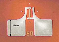
The flexible silicon strain gauge is shown in Photo 1. In its simplest form, the single-crystal or polycrystalline silicon member is a rectangle, aligned to the direction of measured strain, with typical dimensions 20 by 2 mils (500 by 50 mm). The leadwire attachment pads on either side of the sensing member are designed with a symmetrical, low-stress geometry to minimize residual stress effects on the silicon bar. They can be either conventional solder pads or wirebond pads; an aluminum surface is typically used for wirebonding, and gold-plated nickel for soldering. Since they are by far the largest feature of the device, the pads determine device size. Users who have the means to attach leads to smaller pads can specify total device areas down to fractions of a square millimeter.
|
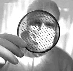
A rugged, low-stress polyimide backing similar to Kapton tape supports the entire structure, whose total thickness is typically <1 mil. Because the element and pad structures are foil thin, the entire strain gauge has a bend radius of <0.06 in., allowing instrumentation of curved or irregular surfaces not previously possible with semiconductor gauges.
LN-100 is fabricated by a proprietary process (patent pending) based on advanced silicon micromachining techniques developed for the MEMS industry. The silicon elements, pads, and backing are all batch fabricated (see Photo 2) for uniformity and cost advantages. The
|
gauges are then diced from the polyimide sheet with an ordinary cutting tool.
Variations
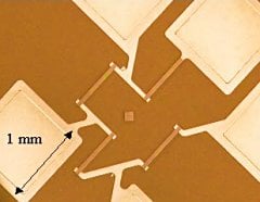
Because it is a MEMS device, the LN-100 takes advantage of the wide range of patterns and geometries available through photolithographic processes such as the Wheatstone bridge layout shown in Photo 3. Rosettes and other patterns are also achievable, with feature tolerances of several microns.
An additional benefit of photolithography is the possibility for integration with standard flex circuit technology. In the example shown in Photo 4, a helicopter research laboratory wished to instrument seven roots of a spur gear. The conventional method required
|
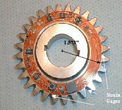
technicians to apply metal foil gauges individually to each root, solder the leads, glue them to the gear surface, and ultimately run them through a slip ring. The setup effort and loss of measurement accuracy brought about by this arrangement were significant, and are typical of the challenges encountered by strain gauge users.
We developed a single-flex circuit, with flip-down tabs at the seven measurement points, to attach to the gear. The battery-powered circuit, which resides on the gear face, contains signal conditioning, A/D conversion, and RF transmission electronics. The solder pads for the circuit components interconnect directly to the strain gauges on the tabs. Now the user has one alignment step instead of seven, no gauge soldering or wire fixation, and no slip rings.
|
||||||||||||
Performance Parameters
Table 1 summarizes typical performance parameters from preproduction lots of LN-100s fabricated from p-type single-crystal silicon. Experimental lots have also been made of polysilicon and n-type single-crystal silicon. As expected, the n-type devices exhibit negative gauge factors in the range of –17 to –30. The polysilicon gauges thus trade lower gauge factor for slightly better temperature coefficient.
As with metal foil gauges, the nominal gauge resistance can be adjusted by varying geometrical parameters in the photolithographic mask. Resistance values of 100–10,000 V are theoretically possible.
Gauge factor is a function of the doping level and concentration, and is also highly dependent on the procedure used to affix the gauges to the test specimen, as discussed below. Whatever the adhesion method, the response of LN-100 gauges is linear under both tension and compression (see Figure 1).
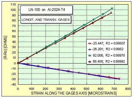 Figure 1. The relative change in resistance as a function of strain is plotted for gauges positioned along and perpendicular to the test beam's axis. The insets summarize the unstrained resistance values, typical sensitivities (gauge factors), and linear correlation coefficients for complete strain cycles. The magnitude of the latter parameter clearly indicates insignificant hysteresis errors. |
At the present stage of development, LN-100s made of single-crystal silicon exhibit a relatively high transverse-to-longitudinal sensitivity factor, Kt, defined by:
|
|
(1) |
where:
| ΔR | = (R-R0) = change in resistance due to strain |
| R0 | = unstrained gauge's resistance |
Measured values are typically about –20%, but methods of reducing longitudinal sensitivity are being developed to make these devices attractive for stress-strain field analysis.
Application Procedure
LN-100s can be applied to substrates with the same adhesives used on conventional metal foil strain gauges, but the application procedure has a more significant effect on high-sensitivity silicon gauges than it does on conventional types.
Figure 2 plots typical gauge factor measurement curves for similar gauges attached to Al-2024-T4 specimens, but with two different adhesive solutions.
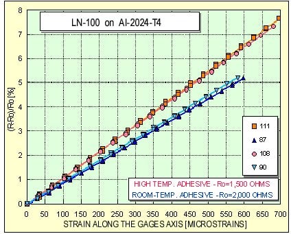 Figure 2. In a plot of the typical variation of the LN-100's gauge factor as influenced by the adhesion procedure, each set of lines represents a different adhesive and cure time. |
For gauges affixed at room temperature (with a fast-curing adhesive), the typical gauge factor is ~88; for gauges attached with a high-temperature (200°C) curing adhesive, the corresponding gauge factor is near 110.
Furthermore, the use of high-temperature epoxies to affix the gauges changes the resistance values from their preattached (nominal) values because of the different thermal expansion coefficients of silicon and the specimen. After curing, the resistance is typically reduced from its original value by 15%–20%. Such resistance variations are not observed when room-temperature curing adhesives are used. We are now developing an application protocol that optimizes gauge factor and repeatability.
Applications and Future Work
Preliminary beta market testing of LN-100s among load cell manufacturers and users is under way. The obvious advantage of a high-sensitivity strain gauge is the increased precision it allows load cell makers to offer their customers. Other, less obvious advantages are being reported as well. The increased gauge sensitivity reduces the sensitivity requirement on the load cell, allowing manufacturers to use less-sensitive, more robust load cells in applications where strength or crashworthiness is critical. Dual-function load cells, which measure strain and also serve a structural function in the end system, become practical. Finally, with increased DR, load cell manufacturers can often obtain the desired strain sensitivity with greatly simplified signal conditioning circuitry and calibration protocols. It is hoped that a high-sensitivity, easy-to-use gauge will enable new breakthroughs in load cell technology.
Ongoing work is focused on reducing the gauges' thermal output, as well as matching their TCR with the substrate's temperature coefficient of expansion. Initial results are promising, as shown in Figure 3 where the thermal output (i.e., apparent strain) of LN-100s is given for typical gauges ("uncompensated" curve) and those optimized for low-TCR ("compensated" curve). Other efforts are focused on development of a special single-crystal silicon gauge with 0% transverse sensitivity.
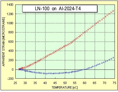 Figure 3. Work is in progress to reduce the LN-100's thermal output and match its temperature coefficient of resistance with the substrate's temperature coefficient of expansion. |
Summary
A silicon strain gauge as easy to handle and use as a metal foil gauge has been demonstrated to have gauge factors as high as 110, a 0.06 in. bend radius, integrated solder pads, and compatibility with conventional mounting methods. Additional benefits include relatively low-cost manufacture and direct integration with flex circuitry. This type of strain gauge could find wide application in the load cell and weigh scale industry. A temperature-compensated version is under development.
References
1. Transducer Catalog #305. 1987. "Forward," BLH Inc.
2. H.L. Trietley. 1986. Transducers in Mechanical and Electronic Design, M. Dekker, Inc., NY:59.