
 | |
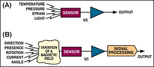
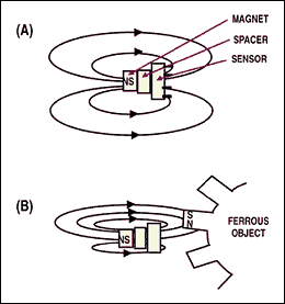
| Figure 1. Conventional sensors detect a physical property directly (A); magnetic sensors detect changes in magnetic fields and from them derive information on physical properties (B). |
Magnetic sensors can be classified according to low-, medium-, and high-field sensing range. In this article, devices that detect magnetic fields <1 µG (microgauss) are considered low-field sensors; those with a range of 1 µG to 10 G are Earth's field sensors; and detectors that sense fields >10 G are referred to as bias magnet field sensors. Table 1 lists magnetic sensor technologies and their sensing ranges [1].
| Magnetic Sensor Technology |
DETECTABLE FIELD RANGE (gauss)*
| ||||||||
|
SQUID
FIBER-OPTIC OPTICALLY PUMPED NUCLEAR PRECESSION SEARCH-COIL
ANISOTROPIC MAGNETORESISTIVE
|
 |
A magnetic field is a vector quantity with both magnitude and direction.
The scalar sensor measures the field's total magnitude but not its direction.
The omnidirectional sensor measures the magnitude of the component of magnetization
that lies along its sensitive axis. The bidirectional sensor includes direction
in its measurements. The vector magnetic sensor incorporates two or three
bidirectional detectors. Some magnetic sensors have a built-in threshold
|
Unit Conversion from SI to Gaussian 79.6 A/m = 1 oersted 100 microtesla = 1 gauss 1 gauss = 1 oersted (in free air) 1 gauss = 10-4 tesla = 105 gamma 1 nanotesla = 10 microgauss = 1 gamma |
Low-Field Sensors
Low-field sensors tend to be bulky and costly compared to other magnetic
devices. Care must be taken to account for the effects of the Earth's field,
whose daily variations may exceed the sensor's measurement range. The devices
are used for medical applications and military surveillance.
SQUID. The most sensitive low-field sensor is the superconducting quantum interference device (SQUID). Developed about 1962, it is based on Brian J. Josephson's work on the point-contact junction designed to measure extremely low currents [1]. SQUID magnetometers can detect fields from several femtotesla up to 9 tesla, a range of more than 15 orders of magnitude. This is essential in medical applications since the neuromagnetic field of the human brain is only a few tenths of a femtotesla [2]; Earth's magnetic field, by way of comparison, is ~50 microtesla, or 0.5 oersted. SQUIDs require cooling to liquid helium temperature (4 kelvin) at present, but devices are under development that will operate at higher temperatures.
Search-Coil. The basic search-coil magnetometer is based on Faraday's law of induction, which states that the voltage induced in a coil is proportional to the changing magnetic field in the coil. This induced voltage creates a current that is proportional to the rate of change of the field. The sensitivity of the search-coil is dependent on the permeability of the core and the area and number of turns of the coil. Because search-coils work only when they are in a varying magnetic field or moving through one, they cannot detect static or slowly changing fields. Inexpensive and easily manufactured, the devices are commonly found in the road at traffic control signals.
Other Low-Field Sensors. Other low-field sensor technologies include nuclear precession, optically pumped, and fiber-optic magnetometers. These precision instruments are used in laboratories and medical applications. For instance, the long-term stability of the nuclear precession magnetometer can be as low as 50 pT/yr. These magnetometers will not be discussed in this article.
Earth's Field (Medium-Field) Sensors The magnetic range of medium-field sensors lends itself well to using the Earth's magnetic field to determine compass headings for navigation, detect anomalies in it for vehicle sensing, and measure the derivative of the change in field to determine yaw rate.Flux Gate. The flux-gate magnetometer, the most widely used sensor for compass-based navigation systems, was developed about 1928 and later refined by the military for submarine detection. The devices have also been used for geophysical prospecting and airborne magnetic field mapping operations.
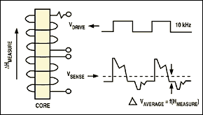 | |
| Figure 2. The most common type of flux-gate magnetometer consists of two coils wrapped around a common high-permeability ferromagnetic core whose magnetic induction changes in the presence of an external magnetic field. |
A well-designed flux-gate magnetometer can sense a signal in the tens of microgauss range, as well as measure both magnitude and direction of static magnetic fields. The upper frequency band limit is ~1 kHz due to the drive frequency limit of ~10 kHz. These devices tend to be bulky and not so rugged as smaller, more integrated sensor technologies.
Magnetoinductive. Magnetoinductive magnetometers are relatively new, with the first patent issued in 1989. This sensor is simply a single winding
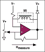 | |
| Figure 3. A magnetoinductive sensor is simply a single winding coil in a ferromagnetic core that changes permeability within the Earth's field. |
Anisotropic Magnetoresistive (AMR). William Thompson, later Lord Kelvin [6], first observed the magnetoresistive effect in ferromagnetic metals in 1856. His discovery had to wait more than 100 years before thin film technology could make it into a practical sensor. Magnetoresistive sensors come in a variety of shapes and forms and are used in high-density read heads for tape and disk drives, as well as for automotive wheel speed and crankshaft measurement, compass navigation, vehicle detection, and current sensing.
AMR sensors are well suited to measuring both linear and angular position and displacement in the Earth's magnetic field. These devices are made of
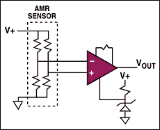 | |
| Figure 4. Anisotropic magnetoresistive sensors, used to measure linear and angular position and displacement in the Earth's magnetic field, are made of a nickel-iron thin film deposited on a silicon wafer and patterned as a resistive strip. |
AMR sensors can be bulk manufactured on silicon wafers and mounted in commercial IC packages, permitting automated assembly with other circuit
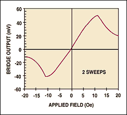 | |
| Figure 5. Anisotropic magnetoresistive sensors offer high sensitivity, small size, and immunity to noise. |
A detailed explanation of AMR technology will be published in the March 1999 issue of Sensors.
Bias Magnetic Field SensorsMost industrial sensors use permanent magnets as a source of the magnetic field to be detected. These magnets magnetize, or bias, ferromagnetic objects close to the sensor, which then detects changes in the total field around itself. Bias field sensors must detect fields that are typically larger than the Earth's, but must not be temporarily upset or permanently affected by a large field. Sensors in this category include reed switches, InSb magnetoresistors, Hall devices, and GMR sensors. Although some of these sensors, such as magnetoresistors, are capable of measuring fields up to several teslas, others, such as GMR devices, can detect fields down to the milligauss region with research extending their capabilities to the microgauss region.
Reed Switches. The reed switch can be considered the simplest magnetic sensor to produce a usable output for industrial control. It consists of a pair of flexible, ferromagnetic contacts hermetically sealed in an inert gas filled container, often glass. The magnetic field along the long axis of the contacts magnetizes the contacts and causes them to attract each other, closing the circuit. Because there is usually considerable hysteresis between the closing and releasing fields, the switches are quite immune to small fluctuations in the field.
Reed switches are maintenance free and highly immune to dirt and contamination. Rhodium-plated contacts ensure long contact life. Typical capabilities are 0.1-0.2 A switching current and 100-200 V switching voltage. Contact life is measured at 106-107 operations at 10 mA. Reed switches are available with normally open, normally closed, and class C contacts. Latching reed switches are also available. Mercury-wetted reed switches can switch currents as high as 1 A and have no contact bounce.
Low cost, simplicity, reliability, and zero power consumption make reed switches popular in many applications. The addition of a separate small permanent magnet yields a simple proximity switch often used in security systems to monitor the opening of doors or windows. The magnet, affixed to the movable part, activates the reed switch when it comes close enough. The desire to sense almost everything in cars is increasing the number of reed switch sensing applications in the automotive industry.
Lorentz Force Devices. There are several sensors that use the Lorentz force, or Hall effect, on charge carriers in a semiconductor. The Lorentz force equation describes the force FL experienced by a charged particle with charge q moving with velocity v in a magnetic field B:
FL = q (v × B)
Since FL, v, and B are vector quantities, they have both magnitude and direction. The Lorentz force is proportional to the cross product between the vectors representing velocity and magnetic field; it is therefore perpendicular to both of them and, for a positively charged carrier, has the direction of advance of a right-handed screw rotated from the direction of v toward the direction of B. The acceleration caused by the Lorentz force is always perpendicular to the velocity of the charged particle; therefore, in the absence of any other forces, a charge carrier follows a curved path in a magnetic field.
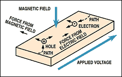 | |
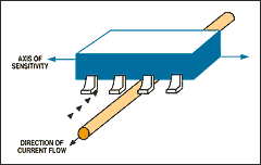
| Figure 6. The Hall effect is illustrated by a semiconductor slab showing magnetic field, applied voltage, forces on electrons and holes, and paths of electrons and holes. |
The Hall effect is a consequence of the Lorentz force in semiconductor materials. When a voltage is applied from one end of a slab of semiconductor material to the other, charge carriers begin to flow. If at the same time a magnetic field is applied perpendicular to the slab, the current carriers are deflected to the side by the Lorentz force. Charge builds up along the side until the resulting electrical field produces a force on the charged particle sufficient to counteract the Lorentz force. This voltage across the slab perpendicular to the applied voltage is called the Hall voltage (see Figure 6).
Magnetoresistors. The simplest Lorentz force devices are magnetoresistors that use semiconductors such as InSb and InAs with high room-temperature carrier mobility. If a voltage is applied along the length of a thin slab of semiconductor material, a current will flow and a resistance can be measured. When a magnetic field is applied perpendicular to the slab, the Lorentz force will deflect the charge carriers. If the width of the slab is greater than the length, the charge carriers will cross the slab without a significant number of them collecting along the sides. The effect of the magnetic field is to increase the length of their path and, thus, the resistance. An increase in resistance of several hundred percent is possible in large fields. To produce sensors with hundreds to thousands of ohms of resistance, long, narrow semiconductor stripes a few micrometers wide are produced using photolithography. The required length-to-width ratio is accomplished by forming periodic low-resistance
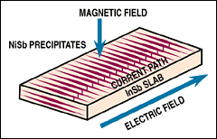 | |
| Figure 7. Magnetoresistors can be built of boules with needle-shaped low-resistance precipitates of NiSb in a matrix of InSb. The precipitates serve as the shorting bars. |
A second method is to use lapped wafers cut from boules that have needle-shaped low-resistance precipitates of NiSb in a matrix of InSb. These precipitates serve as the shorting bars [9]. In Figure 7, which shows the effect of these shorting bars on the current path, notice that the higher the magnetic field, the longer the current path and the higher the resistance.
Magnetoresistors formed from InSb are relatively insensitive in low fields; in high fields, however, they exhibit a resistance that changes approximately as the square of the field. They are sensitive only to that component of the magnetic field perpendicular to the slab and not to whether the field is positive or negative. Their large temperature coefficients
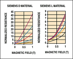 | |
| Figure 8. Resistance is plotted against field for an InSb magnetoresistor at temperatures of 20ºC, 0ºC, 25ºC, 60ºC, 90ºC, and 120ºC (top to bottom). Resistance is normalized to the resistance at zero field. |
Hall sensors. Hall sensors typically use n-type silicon when cost is of primary importance and GaAs for higher temperature capability due to its larger band gap. In addition, InAs, InSb, and other semiconductor materials are gaining popularity due to their high carrier mobilities that result in greater sensitivity and frequency response capabilities above the 10-20 kHz typical of Si Hall sensors. Compatibility of the Hall sensor material with semiconductor substrates is important since Hall sensors are often used in integrated devices that include other semiconductor structures.
A Hall sensor uses a geometry similar to that shown in Figure 6; in this case, however, the length in the direction of the applied voltage is greater than the width. Charge carriers are deflected to the side and build up until they create a Hall voltage across the slab with a force equaling the Lorentz force on the charge carriers. At this point the charge carriers travel the length in approximately straight lines, and no additional charge builds up. Since the final charge carrier path is essentially along the applied electric field, the end-to-end resistance changes little with the magnetic field. When the Hall voltage is measured between electrodes placed at the
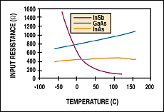 | |
| Figure 9. Three Hall effect sensors made of different semiconductor materials exhibit input resistances that change with temperature. |
The Hall resistance and Hall voltage increase linearly with applied field to several teslas (tens of kilogauss). The temperature dependence of the voltage and the input resistance is governed by the temperature dependence
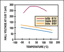 | |
| Figure 10. The Hall voltage at 0.05 T (500 Oe) of several Hall sensors made of different semiconductor materials is plotted vs. temperature. The input voltage is given for each material. |
Integrated Hall sensors. Hall devices are often combined with semiconductor elements to create integrated sensors. Adding comparators and output devices to a Hall element, for example, yields unipolar and bipolar digital switches. Adding an amplifier increases the relatively low voltage signals from a Hall device to produce ratiometric linear Hall sensors with an output centered on one-half the supply voltage. Power usage can even be reduced to extremely low levels by using a low duty cycle [11].
Giant Magnetoresistive (GMR) Devices. Large magnetic field dependent changes in resistance are possible in thin film ferromagnet/nonmagnetic metallic multilayers. The phenomenon was first observed in France in 1988 [12], when changes in resistance with magnetic field of up to 70% were seen. Compared to the small percent change in resistance observed in anisotropic magnetoresistance, this phenomenon was truly giant magnetoresistance.
The resistance of two thin ferromagnetic layers separated by a thin nonmagnetic conducting layer can be altered by changing the moments of the ferromagnetic layers from parallel to antiparallel, or parallel but in the opposite direction.
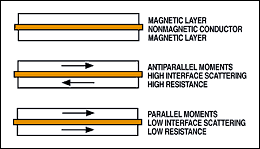 | |
| Figure 11. In a giant magnetoresistive sensor, the resistance of two thin ferromagnetic layers separated by a thin nonmagnetic conducting layer can be altered by changing the moments of the ferromagnetic layers from parallel to antiparallel. |
Various methods of obtaining antiparallel magnetic alignment in thin ferromagnet-conductor multilayers have been discussed elsewhere [13-15]. The structures currently used in GMR sensors are unpinned sandwiches and antiferromagnetic multilayers, although spin valves are of considerable interest especially for magnetic read heads.
Unpinned sandwich GMR materials consist of two soft magnetic layers of iron, nickel, and cobalt alloys separated by a layer of a nonmagnetic conductor such as copper. With magnetic layers 4-6 nm (40-60 Å) thick separated by a conductor layer typically 3-5 nm thick, there is relatively little magnetic coupling between the layers. For use in sensors, the sandwich material is usually patterned into narrow stripes. The magnetic field caused by a current of a few milliamps per micrometer of stripe width flowing along the stripe is sufficient to rotate the magnetic layers into antiparallel or high-resistance alignment. An external field of 3-4 kA/m (35-50 Oe) applied along the length of the stripe is sufficient to overcome the field from the current and rotate the magnetic moments of both layers parallel to the external field. A positive or negative external field parallel to the stripe will also produce the same change in resistance. An external field applied perpendicular to the stripe will have little effect due to the demagnetizing fields associated with the extremely narrow dimensions
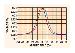 | |
| Figure 12. Voltage is plotted against applied field for a 2 mm wide stripe of unpinned sandwich GMR material with 1.5 mA current. GMR = 5%. |
Antiferromagnetic multilayers consist of multiple repetitions of alternating conducting magnetic and nonmagnetic layers. Because multilayers have more interfaces than do sandwiches, the size of the GMR effect is larger. The thickness of the nonmagnetic layers is less than that for sandwich material (typically 1.5-2.0 nm), and it is critical. For certain thicknesses only, the polarized conduction electrons cause antiferromagnetic coupling between the magnetic layers. Each magnetic layer has its magnetic moment antiparallel to the moments of the magnetic layers on each side exactly the condition needed for maximum spin-dependent scattering. A large external field can overcome the coupling that causes this alignment, and can align
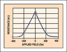 | |
| Figure 13. Resistance is plotted against applied field for a 2 mm wide stripe of antiferromagnetically coupled multilayer GMR material. GMR = 14%. |
In the plot of resistance vs. applied field for a multilayer GMR material shown in Figure 13, note the higher GMR value, typically 12%-16%, and the much higher external field required to saturate the effect, typically 20 kA/m (250 Oe). Multilayer GMR materials have better linearity and lower hysteresis than typical sandwich GMR material.
Spin valves, or antiferromagnetically pinned spin valves, are similar to the unpinned spin valves or sandwich materials described above. An additional layer of an antiferromagnetic material is provided on the top or the bottom. The antiferromagnetic material such as FeMn or NiO couples to the adjacent magnetic layer and pins it in a fixed direction; the other magnetic layer is free to rotate. These materials do not require the field from a current to achieve antiparallel alignment or a strong antiferromagnetic exchange coupling to adjacent layers. The direction of the pinning layer is usually fixed by elevating the temperature of the GMR structure above the blocking temperature. Above this temperature, the antiferromagnet is no longer coupled to the adjacent magnetic layer. The structure is then cooled in a strong magnetic field that fixes the direction of the moment of the pinned layer. Because the spin valve material looses its orientation if heated above its blocking temperature, spin valve sensors must operate below that temperature. Since the change in magnetization in the free layer is due to rotation rather than domain wall motion, hysteresis is reduced. Values for GMR are 4%-20% and saturation fields are 0.8-6 kA/m (10-80 Oe).
Spin valves are receiving considerable interest from the research community due to their potential for use in magnetic read heads for high-density data storage applications [16]. IBM has announced the introduction of a 16.8 GB hard drive with a spin valve read head. Bridge sensor designs using spin valve materials have also been described in the literature [17] and rotational position sensors in a product bulletin [18].
Spin-dependent tunneling (SDT) structures are very similar to those shown in Figure 11. The difference is that an extremely thin insulating layer is substituted for the conductive interlayer separating the two magnetic layers. The conduction is due to quantum tunneling through the insulator. The size of the tunneling current between the two magnetic layers is modulated by the direction between the magnetization vectors in the two layers [19]. The conduction path must be perpendicular to the plane of the GMR material since there is such a large difference between the conductivity of the tunneling path and that of any path in the plane. Extremely small SDT devices measuring several micrometers on a side with high resistance can be fabricated using photolithography, which allows very dense packing of magnetic sensors in small areas. Although these recent materials are very much a topic of current research, values of GMR of 10%-25% have been observed. The saturation fields depend on the composition of the magnetic layers and the method of achieving parallel and antiparallel alignment. Values of saturation field range from 0.1 kA/m to 10 kA/m (1-100 Oe), offering the possibility of extremely sensitive magnetic sensors with very high resistance that promise to be suitable for battery operation.
Colossal magnetoresistance. Scientists, to surpass the term giant, have proceeded on to colossal magnetoresistive materials (CMR). Under certain conditions these mixed oxides undergo a semiconductor-to-metallic transition with the application of a magnetic field of a few teslas (tens of kilogauss). The size of the resistance ratios, measured at 103%-108%, have generated considerable excitement even though they initially required high fields and liquid nitrogen temperatures. Academic researchers have recently developed CMR materials that work at room temperature and have fabricated Wheatstone bridge topography sensors out of these materials [20]. Although still a long way from commercial applications, these CMR materials bear watching.
GMR Circuit Techniques. The best use of GMR materials for magnetic
field sensors has so far been in Wheatstone bridge configurations, although
simple GMR resistors and GMR half bridges can also be fabricated. A sensitive
bridge can be made from four photolithographically patterned GMR resistors,
two of which are active elements. These resistors can be as narrow as 2
µm, allowing a serpentine 10 ![]() k resistor to be patterned in an area as small
as 100 µm2. The vary narrow width also makes the resistors sensitive only
to the magnetic field component along their long dimension. Small magnetic
shields are plated over two of the four equal resistors in a Wheatstone
bridge, protecting them from the applied field and allowing them to act
as reference resistors. Since they are fabricated from the same material,
they have the same temperature coefficient as the active resistors. The
two remaining GMR resistors are both exposed to the external field. The
bridge output is therefore twice the output from a bridge with only one
active resistor. The bridge output for a 10% change in these resistors is
~5% of the voltage applied to the bridge.
k resistor to be patterned in an area as small
as 100 µm2. The vary narrow width also makes the resistors sensitive only
to the magnetic field component along their long dimension. Small magnetic
shields are plated over two of the four equal resistors in a Wheatstone
bridge, protecting them from the applied field and allowing them to act
as reference resistors. Since they are fabricated from the same material,
they have the same temperature coefficient as the active resistors. The
two remaining GMR resistors are both exposed to the external field. The
bridge output is therefore twice the output from a bridge with only one
active resistor. The bridge output for a 10% change in these resistors is
~5% of the voltage applied to the bridge.
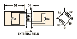 | |
| Figure 14. GMR resistors can be configured as a Wheatstone bridge sensor. In the flux concentrators shown here, D1 is the length of the gap between the flux concentrators and D2 is the length of one flux concentrator. |
Additional Permalloy structures are plated onto the substrate to act as flux concentrators. The active resistors, placed in the gap between two flux concentrators (see Figure 14), experience a field that is larger than the applied field by approximately the ratio of the gap between the flux concentrators, D1, to the length of one of the flux concentrators, D2. In some sensors the flux concentrators are also used as shields by placing two resistors beneath them, as is shown for R2 and R3. The sensitivity of a GMR bridge sensor can be adjusted in design by changing the lengths of the flux concentrators and the size of the gap between them. Thus, a GMR material that saturates at ~300 Oe can be used to build different sensors that saturate at 15 Oe, 50 Oe, and 100 Oe. For sensors with even more sensitivity, external coils and feedback can be used to produce resolution in the 100 mA/m or millioersted range.
Smart sensors with sensing elements and associated electronics such as amplification and signal conditioning on the same die are the latest trend. GMR materials are sputtered onto wafers and can therefore be directly integrated with semiconductor processes. The small sensing elements fit well with the other semiconductor structures and are applied after most of the semiconductor fabrication operations are complete. Because of the topography introduced by the many layers of polysilicon, metal, and oxides over the transistors, areas must be reserved with no underlying transistors or connections. These areas will have the GMR resistors. The GMR materials are actually deposited over the entire wafer, but the etched sensor elements remain only on these reserved, smooth areas on the wafers [21].
Among the functions built into an integrated sensor are regulated voltage or current supplies to the sensor elements; threshold detection to provide a switched output when a preset field is reached; amplifiers; logic functions, including divide-by-2 circuits; and various options for outputs. With these elements, a 2-wire sensor can be designed that has two current levels low when the field is below a threshold and high when the field is above the threshold.
Onboard sensor electronics can increase signal levels to significant voltages with the least pickup of interference. It is always best to amplify
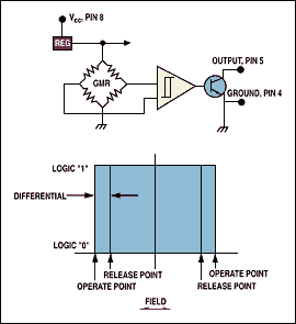 | |
| Figure 15. The schematic and logic output characteristic of a commercial integrated digital GMR sensor is illustrated. |
GMR materials have been successfully integrated with both BiCMOS and bipolar semiconductor underlayers. The wafers are processed with all but the final layer of connections complete. GMR material is deposited on the surface and patterned. The next step is the application of a passivation layer through which windows are cut to permit contact to both the upper metal layer in the semiconductor wafer and to the GMR resistors. The final layer of metal is then deposited and patterned to interconnect the GMR sensor elements and to connect them to the semiconductor underlayers. This layer also forms the pads to which wires will be bonded during packaging. A final passivation layer is deposited, magnetic shields and flux concentrators are plated and patterned, and windows are etched through to the pads.
GMR Sensor ApplicationsProximity Detection. A magnetic field sensor can directly detect a magnetic field from a permanent magnet, an electromagnet, or a current. Ferrous object presence sensing often entails the use of a biasing magnet that magnetizes a ferromagnetic object such as a gear tooth. The sensor then detects the combined magnetic fields from the object and the magnet. To keep its direct influence on the target to a minimum, the magnet is usually mounted on top of the sensor with its magnetic axis perpendicular to the sensitive axis of the sensor. Centering the biasing magnet such that there
 | |
| Figure 16. In a GMR configuration designed for proximity detection, the biasing magnet and sensor in an 8-pin package are shown in side view with and without the presence of a ferrous object. |
Biasing magnets are customarily used only if the ferrous object is nearby. Because the field from a dipole magnet falls off at the reciprocal of the distance cubed, it is difficult to magnetize an object several meters away with the field from a sensor-sized permanent magnet. In vehicle detection and certain other applications, the Earth's field acts as a biasing magnet and creates a magnetic signature from the parts of the vehicle that are magnetized by the Earth's field. Vehicles can thus be counted and classified as they pass over sensors in the road. Small, low-power GMR sensors and their associated electronics, memory, and battery can be packaged in a low-profile aluminum housing the size of a hand [22].
Currency detection is another application in which the biasing magnet is not mounted on the sensor. The particles in the ink on many countries' currency have ferromagnetic properties. Bills are passed over a permanent magnet array and magnetized along their direction of travel. A magnetic sensor located several inches away with its sensitive axis parallel to the direction of travel can detect the remnant field of the ink particles. The purpose of the biasing magnet in this case is to achieve a controlled orientation of the magnetic moments of the ink particles, resulting in a maximum and recognizable magnetic signature. Reversing the magnetizing field can actually invert the signature.
Displacement Sensing. GMR bridge sensors can provide position information from small displacements associated with actuating components
 | |
| Figure 17. GMR sensors are shown as positioned to measure displacement relative to a permanent dipole magnet. The sensitive axes are indicated and the component of field along the sensitive axes for the two sensors is plotted. |
Rotational Reference Detection. GMR sensors offer a rugged, low-cost solution to rotational reference detection. High sensitivity and DC operation afford the GMR bridge sensor an advantage over inductive sensors, which tend to have very low outputs at low frequencies and can generate large noise signals when subjected to high-frequency vibrations. Because GMR sensors are field sensors, they do not measure the induced signal from the time rate of change of fields as is the case with variable reluctance sensors. The output from a GMR bridge sensor will have a minimum when the sensor is centered over a tooth or a gap and a maximum when a tooth approaches or recedes. The bridge sensor shown in Figure 16 is in position for angular position sensing.
Current Sensing. Current in a wire creates a magnetic field that surrounds the wire or a trace on a PCB. The field decreases as the reciprocal of distance from the wire; GMR bridge sensors can be used to detect this field and thus either DC or AC currents. Bipolar AC current will be rectified
 | |
| Figure 18. A GMR bridge sensor is oriented as shown to detect the magnetic field created by a current-carrying wire. |
Magnetic field detection has vastly expanded as industry has used a variety of magnetic sensors to detect the presence, strength, or direction of magnetic fields from the Earth, permanent magnets, magnetized soft magnets, and the magnetic fields associated with current. These sensors are used as proximity sensors, speed and distance measuring devices, navigation compasses, and current sensors. They can measure these properties without actual contact to the medium being measured and have become the eyes of many control systems.
References
1. J.E. Lenz. June 1990. "A Review of Magnetic Sensors," Proc
IEEE, Vol. 78, No. 6:973-989.
2. H. Yabuki. "Quasi-Planar SNS junction as a Sensor for Brain Studies, " Riken-The Institute of Physical and Chemical Research, www.riken.go.jp/Yoran/BSIS/140B-141.html
3. J.M. Janicke. 1994. The Magnetic Measurement Handbook, New Jersey: Magnetic Research Press.
4. P. Ripka. 1996. "Review of Fluxgate Sensors," Sensors and Actuators A, 33:129-141.
5. E. Ramsden. Sept. 1994. "Measuring Magnetic Fields with Fluxgate Sensors," Sensors:87-90.
6. P. Ciureanu and S. Middelhoek. 1992. Thin Film Resistive Sensors, New York: Institute of Physics Publishing.
7. B.B. Pant. Fall 1987. "Magnetoresistive Sensors," Scientific Honeyweller, Vol. 8, No. 1:29-34.
8. J.E. Lenz et al. 1992. "A Highly Sensitive Magnetoresistive Sensor," Proc Solid State Sensor and Actuator Workshop.
9. Magnetic Sensors International Data Book. 1995. Siemens Aktiengesellschaft, München, Germany.
10. Hall Element (data sheet). Ashai Kassi Electronics Co., Ltd., 1-1-1 Uchisaiwai-Cho, Chiyoda-Ku, Tokyo 100, Japan.
11. Paul Emerald. March 1998. "Low Duty Cycle Operation of Hall Effect Sensors for Circuit Power Conservation," Sensors, Vol. 15, No. 3:38.
12. M.N. Baibich et al. 1988. "Giant Magnetoresistance of (001)Fe/(001)Cr Magnetic Superlattices," Phys Rev Lett, Vol. 61: 2472-2475.
13. Carl H. Smith and Robert W. Schneider. 1997. "Expanding The
Horizons Of Magnetic Sensing: GMR," Proc Sensors Expo Boston:139-144.
14. J. Daughton and Y. Chen. 1993. "GMR Materials for Low Field Applications," IEEE Trans Magn, Vol. 29:2705-2710.
15. J. Daughton et al. 1994. "Magnetic Field Sensors Using GMR Multilayer," IEEE Trans Magn, Vol. 30:4608-4610.
16. C. Tsang et al. 1994. "Design, fabrication and testing of spin-valve read heads for high density recording," IEEE Trans Magn, Vol. 30:3801-3806.
17. J.K. Spong et al. 1996. "Giant Magnetoresistive Spin Valve Bridge Sensor," IEEE Trans Magn, Vol. 32:366-371.
18. "Preliminary Datasheet for Giant Magneto Resistive Position Sensor." 1997. Siemens Aktiengesellschaft, München, Germany.
19. J. Moodera and L. Kinder. 1996. "Ferromagnetic-insulator-ferromagnetic tunneling: Spin-dependent tunneling and large magnetoresistance in trilayer junctions," J Appl Phys Vol. 79, No. 8:4724-4729.
20. "New materials show no resistance to success." Jan. 1998. Eureka Transfers Technology:26.
21 J.L. Brown. Jan. 1995. "High Sensitivity Magnetic Field Sensor Using GMR Materials with Integrated Electronics," Proc Symp on Circuits and Systems, Seattle, WA.
22. "Tiny Sensor Measures Vehicle's Speed." 1998. nu-metrics News Release, www.nu-metrics.com