

Smaller form factor, excellent functionality, improved performance and lower bill of material (BOM) are the key challenges for system engineers developing complex electronic products such as sensor and sensor interface applications. While die size reduction can be realized by using smaller process nodes with higher integration densities, a system miniaturization can be achieved by using advanced packaging technologies. The increasing demand for higher system integration has pushed the traditional assembly service providers but also the semiconductor companies to develop more innovative and more advanced packaging technologies.
One of the most promising and but also challenging technologies is the 3-dimensional integration of integrated circuits (3DIC) using through Silicon Vias (TSV). 3DIC technology is now widely used in digital ICs (e.g. stacking of memory ICs, image sensors, and others), its design and manufacturing approach has been successfully proven in the digital world. So how can 3DIC technology be successfully implemented in analog and mixed-signal dominated sensor ICs?
Currently pioneering analog and mixed-signal IC developers are starting to recognize substantial benefits in implementing analog 3DIC designs. Smart sensor and sensor interface products target various applications in Industry 4.0, Smart Cities or the Internet of Things (IoT). TSV and backside redistribution layer (BRDL) are very useful technologies for the replacement of traditional gold wire bonding in various chip-stacking technologies. 3D integration technologies, in particular specialty analog TSV technologies from leading foundry service providers, in combination with front-side or back-side RDL, offer more functionality in a reduced board footprint, improve performance due to shorter interconnects and achieve a higher level of integration. In particular the small size of the TSV package technology (total height in the range of 0.32 mm) addresses the small form factor requirement in wearable products such as smart watches or smart glasses.
TSV technologies also offer a higher level of flexibility in combining different wafers or technologies: Wafer to wafer stacking of a digital wafer, e.g. manufactured in a 45-nm process, and an analog wafer (e.g. 180 nm), stacking of MEMS devices or photo sensors and photo diode arrays, just to name a few.
Analog 3DIC technologies typically address sensor applications by creating an electrical connection from the front side of a chip to the back side of the IC. In numerous sensor applications such as optical, chemical, gas or pressure sensors, the sensing area is on the CMOS side (top side of the wafer). The most commonly used connection between die and lead frame is wire bonding (figure 1). Independent whether a plastic package is used or the die is directly bonded on the PCB or flex, for certain applications with exposed sensing area, wire bonding is not the ideal solution. Using specialty foundry service providers' proprietary TSV technology, the bond wires can be replaced by using TSVs, a backside RDL and Chip Scale Packaging (WLCSP) (figure 2).
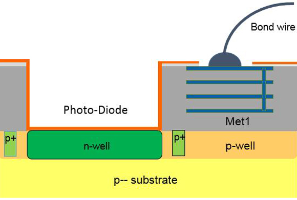
Fig. 1: Sensor chip with standard wire bonding
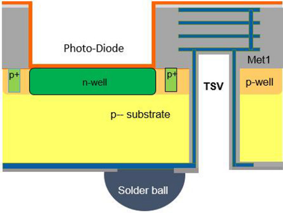
Fig. 2: Sensor chip with backside connection using TSV
Next page
Next Generation TSVs
Similar to semiconductor technologies, where newer process technologies offer higher performance and higher integration density by using smaller geometries and design rules ("Moore's law"), next generation TSV technologies will outperform currently available 3DIC technologies. Some specialty foundry service providers are currently developing their next generation of TSV technologies, which will be significantly smaller in its diameter (approx. 40µm) therefore providing a smaller pitch and higher density while offering the same or even better analog performance. This next generation TSV technology is the base for new 3D applications which foundry service providers are addressing with new service offerings such as so-called "Pad Replacement on 3rd Party Wafers" or "Active 3D Interposers".
Pad Replacement On 3rd Party Wafers
The next generation of Through Silicon Via technology with reduced diameter and pitch will be capable to replace pads of any already processed and completed wafer by using TSVs combined with backside RDL and WLCSP, so-called 3D-WLCSP. Customers will have the flexibility to decide whether the product shall be wire-bonded on the front side or bumped with WLCSP technology on the back side, even after completion of manufacturing process. This new technology concept enables processing of TSVs on any wafer, even 3rd party wafer, as a post processing step (via last concept). The TSV development has been done in a way that its diameter and minimum pitch matches very well the pad requirements of the used process of the third-party wafer (figure 3).
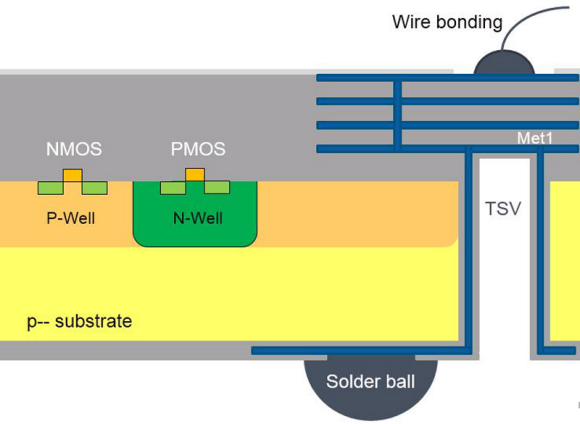
Fig. 3: The wire bond will be replaced by TSV combined with WLCSP (=3D-WLCSP)
3D-Interposer Technology
Another variation and very innovative development of 3DIC technology is the silicon interposer architecture. A so-called passive 3D silicon interposer is used to create a simple electrical connection from the top side to the bottom side of the wafer. The so-called active 3D silicon interposer supports all passive and active devices of a process technology which are required to implement a complete CMOS design.
Leading foundry service provider do offer 3D interposer technologies, which are typically based on 0.18 µm analog specialty processes, featuring various process modules such as MIM caps, high res poly resistor, up to 6 metal layers, thick top metal, and more. The active interposer comes complete with front- and backside pads. While the front side pads are available for the assembly/stacking of any kind of dies such as sensors or MEMS devices, the backside pads are mostly used for board level integration (figure 4). WLCSP technologies with various ball sizes and pitches are offered as additional service by the foundries. Optionally the backside pads can be used to attach further dies to the bottom side.
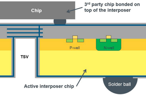
Fig. 4: 3rd party chip bonded on top of the active 3D silicon interposer
Next page
Design Kit Integration
Leading analog foundry service provider do offer their design environment for IC development. Ideally, some very few industry benchmark PDKs do provide all the building blocks required to create complex mixed-signal designs based on the specialty foundry's advanced wafer manufacturing processes and is available for all major state-of-the-art CAD environments. By introducing only minor modifications a 3D integration reference design flow has been established, which allows designers the full functional and physical verification of a 3D integrated IC system. The PDK helps to achieve more efficient designs towards die size, performance, yield and shorter time to market and provides product developers a proven route to "first time right" designs.
Conclusion
3DIC technology is widely used for stacking of memory ICs, image sensors, and others and has been successfully proven in the digital world. Offering advanced 3DIC technologies in analog and mixed-signal dominated applications to their customers is the key challenge for foundry service providers. By shrinking the TSV diameter, reducing the TSV pitch and combining it with Wafer-Level-Chip-Scale technologies, 3D systems architectures become a real alternative to conventional 2D system-in-package solutions. 3DIC concepts such as pad replacement technology or active interposer will significantly improve the system from factor, increase performance and help to reduce the bill of material, which is key in all mobile devices, wearables or smart sensor devices in the IoT domain.
About the Authors
Helmut Hofstaetter is Product Manager at ams AG's Full Service Foundry division. Helmut began his career in semiconductors in 1991 when he joined Austria Mikro Systeme International AG as COT engineer and project manager responsible for foundry customers. He is now leading ams' "More than Silicon" initiative focused on special processes and process IP's and is responsible for tailored customer solutions. Helmut has almost 25 years of experience in semiconductor manufacturing.
Tel: +43 (0) 3136 500 31782
Email: [email protected]
Andreas Wild is Senior Marketing Manager at ams AG's Full Service Foundry division. Andreas began his career in semiconductors in 1995 when he joined Austria Mikro Systeme International AG as an administrator responsible for the product engineering laboratory. Joining the design support team in 1996 Andreas Wild was responsible for PDK qualification, distribution and worldwide technical hotline support. Since 2003 Andreas Wild has been working as Marketing Manager for foundry services and technologies in the Full Service Foundry at ams, and is also responsible for customers in the US and southern Europe.
Tel: +43 (0) 3136 500 31246
Email: [email protected]
Company Info:
Email: [email protected]
URL: http://www.ams.com
Related Stories
AMEC Debuts New Etch Tool
The compact Primo TSV200E is built to provide ultra-high throughput for 200 mm wafer-level packaging, MEMS, and 3DIC applications.
SMIC and Qualcomm Collaborate on 28nm Wafer Production in China